DS26518GN+ Maxim Integrated Products, DS26518GN+ Datasheet - Page 25
DS26518GN+
Manufacturer Part Number
DS26518GN+
Description
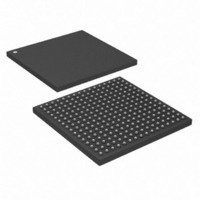
IC TXRX T1/E1/J1 8PORT 256-CSBGA
Manufacturer
Maxim Integrated Products
Type
Transceiverr
Specifications of DS26518GN+
Number Of Drivers/receivers
8/8
Protocol
T1/E1/J1
Voltage - Supply
3.135 V ~ 3.465 V
Mounting Type
Surface Mount
Package / Case
256-CSBGA
Lead Free Status / RoHS Status
Lead free / RoHS Compliant


D5/SPI_SWAP
D6/SPI_CPHA
D7/SPI_CPOL
D2/SPI_SCLK
D1/SPI_MOSI
D0/SPI_MISO
NAME
RDB/
CSB
DSB
A12
A11
A10
A9
A8
A7
A6
A5
A4
A3
A2
A1
A0
D4
D3
C10
B10
A10
PIN
M9
M8
C8
A8
B8
B9
A9
C9
D9
E9
N9
R8
P8
N8
F8
F9
T9
T8
L9
T7
Output
Output
Output
Output
Output
Output
Output
Ouput
TYPE
Input/
Input/
Input/
Input/
Input/
Input/
Input/
Input/
Input
Input
Input
MICROPROCESSOR INTERFACE
Address [12:0]. This bus selects a specific register in the DS26518 during
read/write access. A12 is the MSB and A0 is the LSB.
Data 7/SPI Interface Clock Polarity
D7: Bit 7 of the 8-bit data bus used to input data during register writes and data
outputs during register reads. Not driven when CSB = 1.
SPI_CPOL: This signal selects the clock polarity when SPI_SEL = 1. See Section
9.1.2
Data 6/SPI Interface Clock Phase
D6: Bit 6 of the 8-bit data bus used to input data during register writes and data
outputs during register reads. Not driven when CSB = 1.
SPI_CPHA: This signal selects the clock phase when SPI_SEL = 1. See Section
9.1.2
Data 5/SPI Bit Order Swap
D5: Bit 5 of the 8-bit data bus used to input data during register writes and data
outputs during register reads. Not driven when CSB = 1.
SPI_SWAP: This signal is active when SPI_SEL = 1. The address and data bit
order is swapped when SPI_SWAP is high. The R/W and B bit positions are
never changed in the control word.
Data 4. Bit 4 of the 8-bit data bus used to input data during register writes and
data outputs during register reads. Not driven when CSB = 1.
Data 3. Bit 3 of the 8-bit data bus used to input data during register writes and
data outputs during register reads. Not driven when CSB = 1.
Data 2/SPI Serial Interface Clock
D2: Bit 2 of the 8-bit data bus used to input data during register writes and data
outputs during register reads. Not driven when CSB = 1.
SPI_SCLK: SPI Serial Clock Input when SPI_SEL = 1.
Data 1/SPI Serial Interface Data Master Out-Slave In
D1: Bit 1 of the 8-bit data bus used to input data during register writes, and data
outputs during register reads. Not driven when CSB = 1.
SPI_MOSI: SPI Serial Data Input (Master Out-Slave In) when SPI_SEL = 1.
Data 0/SPI Serial Interface Data Master In-Slave Out
D0: Bit 0 of the 8-bit data bus used to input data during register writes and data
outputs during register reads. Not driven when CSB = 1.
SPI_MISO: SPI Serial Data Output (Master In-Slave Out) when SPI_SEL = 1.
Chip-Select Bar. This active-low signal is used to qualify register read/write
accesses. The RDB/DSB and WRB/ RWB signals are qualified with CSB.
Read Bar/Data-Strobe Bar. This active-low signal along with CSB qualifies read
access to one of the DS26518 registers. The DS26518 drives the data bus with
the contents of the addressed register, in Intel bus mode, while RDB and CSB are
low or, in Motorola bus mode, while DSB and CSB are low and RWB is high.
0 = LSB is transmitted and received first.
1 = MSB is transmitted and received first.
for detailed timing and functionality information. Default setting is low.
for detailed timing and functionality information. Default setting is low.
25 of 312
FUNCTION
Related parts for DS26518GN+
Image
Part Number
Description
Manufacturer
Datasheet
Request
R

Part Number:
Description:
8-port T1/e1/j1 Transceiver
Manufacturer:
Maxim Integrated Products, Inc.
Datasheet:
Part Number:
Description:
Ds26518 8-port T1/e1/j1 Transceiver
Manufacturer:
Maxim Integrated Products, Inc.
Part Number:
Description:
power light source LUXEON� Collimator
Manufacturer:
LUMILEDS [Lumileds Lighting Company]
Datasheet:

Part Number:
Description:
MAX7528KCWPMaxim Integrated Products [CMOS Dual 8-Bit Buffered Multiplying DACs]
Manufacturer:
Maxim Integrated Products
Datasheet:
Part Number:
Description:
Single +5V, fully integrated, 1.25Gbps laser diode driver.
Manufacturer:
Maxim Integrated Products
Datasheet:
Part Number:
Description:
Single +5V, fully integrated, 155Mbps laser diode driver.
Manufacturer:
Maxim Integrated Products
Datasheet:
Part Number:
Description:
VRD11/VRD10, K8 Rev F 2/3/4-Phase PWM Controllers with Integrated Dual MOSFET Drivers
Manufacturer:
Maxim Integrated Products
Datasheet:
Part Number:
Description:
Highly Integrated Level 2 SMBus Battery Chargers
Manufacturer:
Maxim Integrated Products
Datasheet:
Part Number:
Description:
Current Monitor and Accumulator with Integrated Sense Resistor; ; Temperature Range: -40°C to +85°C
Manufacturer:
Maxim Integrated Products
Part Number:
Description:
TSSOP 14/A�/RS-485 Transceivers with Integrated 100O/120O Termination Resis
Manufacturer:
Maxim Integrated Products
Part Number:
Description:
TSSOP 14/A�/RS-485 Transceivers with Integrated 100O/120O Termination Resis
Manufacturer:
Maxim Integrated Products
Part Number:
Description:
QFN 16/A�/AC-DC and DC-DC Peak-Current-Mode Converters with Integrated Step
Manufacturer:
Maxim Integrated Products
Part Number:
Description:
TDFN/A/65V, 1A, 600KHZ, SYNCHRONOUS STEP-DOWN REGULATOR WITH INTEGRATED SWI
Manufacturer:
Maxim Integrated Products
Part Number:
Description:
Integrated Temperature Controller f
Manufacturer:
Maxim Integrated Products