DS26518GN+ Maxim Integrated Products, DS26518GN+ Datasheet - Page 263
DS26518GN+
Manufacturer Part Number
DS26518GN+
Description
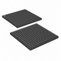
IC TXRX T1/E1/J1 8PORT 256-CSBGA
Manufacturer
Maxim Integrated Products
Type
Transceiverr
Specifications of DS26518GN+
Number Of Drivers/receivers
8/8
Protocol
T1/E1/J1
Voltage - Supply
3.135 V ~ 3.465 V
Mounting Type
Surface Mount
Package / Case
256-CSBGA
Lead Free Status / RoHS Status
Lead free / RoHS Compliant


Register Name:
Register Description:
Register Address:
Bit #
Name
Default
Bit 6: Transmit Packet Start Disable (TPSD). When 0, the transmit packet processor continues sending packets
after the current packet end. When 1, the transmit packet processor stops sending packets after the current packet
end.
Bit 5: Transmit FCS Error Insertion (TFEI). When 0, the calculated FCS (inverted CRC-16) is appended to the
packet. When 1, the inverse of the calculated FCS (noninverted CRC-16) is appended to the packet causing a FCS
error. This bit is ignored if transmit FCS processing is disabled (TFPD = 1).
Bit 4: Transmit Interframe Fill Value (TIFV). When 0, interframe fill is done with the flag sequence (7Eh). When 1,
interframe fill is done with all ones.
Bit 3: Transmit Bit Reordering Enable (TBRE). When 0, bit reordering is disabled. (The first bit transmitted is the
LSB of the transmit FIFO data byte TFD[0]). When 1, bit reordering is enabled. (The first bit transmitted is the MSB
of the transmit FIFO data byte TFD[7]).
Bit 2: Transmit Data Inversion Enable (TDIE). When 0, the outgoing data is directly output from packet
processing. When 1, the outgoing data is inverted before being output from packet processing.
Bit 1: Transmit FCS Processing Disable (TFPD). This bit controls whether a FCS is calculated and appended to
the end of each packet. When 0, the calculated FCS bytes are appended to the end of the packet. When 1, the
packet is transmitted without a FCS.
Bit 0: Transmit FIFO Reset (TFRST). When 0, the transmit FIFO resumes normal operations, however, data is
discarded until a start of packet is received after RAM power-up is completed. When 1, the transmit FIFO is
emptied, any transfer in progress is halted, the FIFO RAM is powered down, and all incoming data is discarded (all
TFDR register writes are ignored).
Register Name:
Register Description:
Register Address:
Bit #
Name
Default
Bits 4 to 0: Transmit HDLC-256 Data Storage Available Level (TDAL[4:0]). These five bits indicate the
minimum number of bytes ([TDAL x 8] + 1) that must be available for storage (do not contain data) in the transmit
FIFO for HDLC-256 data storage to be available. For example, a value of 21 (15h) results in HDLC-256 data
storage being available (THDA = 1) when the transmit FIFO has 169 (A9h) bytes or more available for storage, and
HDLC-256 data storage not being available (THDA = 0) when the transmit FIFO has 168 (A8h) bytes or less
available for storage. Default value (after reset) is 128 bytes minimum available.
—
—
7
0
7
0
TPSD
—
6
0
6
0
TH256CR1
Transmit HDLC-256 Control Register 1
1500h + (20h x (n - 1)) : where n = 1 to 8
TH256CR2
Transmit HDLC-256 Control Register 2
1501h + (20h x (n - 1)) : where n = 1 to 8
TFEI
—
5
0
5
0
TDAL4
263 of 312
TIFV
0
0
4
4
TDAL3
TBRE
3
0
3
1
TDAL2
TDIE
2
0
2
0
TDAL1
TFPD
1
0
1
0
TFRST
TDAL0
0
0
0
0
Related parts for DS26518GN+
Image
Part Number
Description
Manufacturer
Datasheet
Request
R

Part Number:
Description:
8-port T1/e1/j1 Transceiver
Manufacturer:
Maxim Integrated Products, Inc.
Datasheet:
Part Number:
Description:
Ds26518 8-port T1/e1/j1 Transceiver
Manufacturer:
Maxim Integrated Products, Inc.
Part Number:
Description:
power light source LUXEON� Collimator
Manufacturer:
LUMILEDS [Lumileds Lighting Company]
Datasheet:

Part Number:
Description:
MAX7528KCWPMaxim Integrated Products [CMOS Dual 8-Bit Buffered Multiplying DACs]
Manufacturer:
Maxim Integrated Products
Datasheet:
Part Number:
Description:
Single +5V, fully integrated, 1.25Gbps laser diode driver.
Manufacturer:
Maxim Integrated Products
Datasheet:
Part Number:
Description:
Single +5V, fully integrated, 155Mbps laser diode driver.
Manufacturer:
Maxim Integrated Products
Datasheet:
Part Number:
Description:
VRD11/VRD10, K8 Rev F 2/3/4-Phase PWM Controllers with Integrated Dual MOSFET Drivers
Manufacturer:
Maxim Integrated Products
Datasheet:
Part Number:
Description:
Highly Integrated Level 2 SMBus Battery Chargers
Manufacturer:
Maxim Integrated Products
Datasheet:
Part Number:
Description:
Current Monitor and Accumulator with Integrated Sense Resistor; ; Temperature Range: -40°C to +85°C
Manufacturer:
Maxim Integrated Products
Part Number:
Description:
TSSOP 14/A�/RS-485 Transceivers with Integrated 100O/120O Termination Resis
Manufacturer:
Maxim Integrated Products
Part Number:
Description:
TSSOP 14/A�/RS-485 Transceivers with Integrated 100O/120O Termination Resis
Manufacturer:
Maxim Integrated Products
Part Number:
Description:
QFN 16/A�/AC-DC and DC-DC Peak-Current-Mode Converters with Integrated Step
Manufacturer:
Maxim Integrated Products
Part Number:
Description:
TDFN/A/65V, 1A, 600KHZ, SYNCHRONOUS STEP-DOWN REGULATOR WITH INTEGRATED SWI
Manufacturer:
Maxim Integrated Products
Part Number:
Description:
Integrated Temperature Controller f
Manufacturer:
Maxim Integrated Products