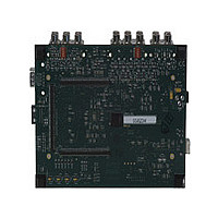
ADDS-BF533-EZLITE Analog Devices Inc, ADDS-BF533-EZLITE Datasheet - Page 13

ADDS-BF533-EZLITE
Manufacturer Part Number
ADDS-BF533-EZLITE
Description
Manufacturer
Analog Devices Inc
Datasheet
1.ADDS-BF533-EZLITE.pdf
(60 pages)
Specifications of ADDS-BF533-EZLITE
Significant Other Parts
ADV7183 Video Decode
Lead Free Status / Rohs Status
Not Compliant
100µF
The power savings factor is calculated as:
where the variables in the equation are:
The percent power savings is calculated as:
VOLTAGE REGULATION
The Blackfin processor provides an on-chip voltage regulator
that can generate appropriate V
V
tor tolerances and acceptable V
Figure 7
complete the power management system. The regulator con
trols the internal logic voltage levels and is programmable with
the voltage regulator control register (VR_CTL) in increments
of 50 mV. To reduce standby power consumption, the internal
voltage regulator can be programmed to remove power to the
processor core while keeping I/O power (V
in the hibernate state, I/O power is still being applied, eliminat
ing the need for external buffers. The voltage regulator can be
activated from this power-down state either through an RTC
wakeup or by asserting RESET, both of which will then initiate a
boot sequence. The regulator can also be disabled and bypassed
at the user’s discretion.
DDEXT
2.25V TO
INPUT VOLTAGE
RANGE
NOTE: DESIGNER SHOULD MINIMIZE
TRACE LENGTH TO FDS9431A.
f
f
V
V
t
t
% power savings = (1 – power savings factor) × 100%
CCLKNOM
CCLKRED
NOM
RED
supply. See
DDINTNOM
DDINTRED
+
LOW ESR
shows the typical external components required to
is the duration running at f
3.6V
10µF
is the duration running at f
power savings factor
= -------------------- - × ------------------------- -
is the reduced core clock frequency
is the nominal core clock frequency
100nF
is the reduced internal supply voltage
f
f
is the nominal internal supply voltage
CCLKNOM
CCLKRED
Figure 7. Voltage Regulator Circuit
Operating Conditions on Page 21
(LOW-INDUCTANCE)
FDS9431A
V
DDEXT
⎛ V
⎝ V
DDINTNOM
DDINTRED
DDEXT
DDINT
ZHCS1000
INDUCTANCE WIRE
SHORT AND LOW-
10µH
ranges for specific models.
voltage levels from the
SET OF DECOUPLING
CCLKRED
CCLKNOM
⎞
⎠
CAPACITORS
100µF
2
× ⎛ ---------- -
100µF
DDEXT
⎝ t
t
+
NOM
RED
+
) supplied. While
⎞
⎠
for regula
Rev. E | Page 13 of 60 | July 2007
V
V
VR
VR
GND
DDEXT
DDINT
OUT
OUT
ADSP-BF531/ADSP-BF532/ADSP-BF533
Voltage Regulator Layout Guidelines
Regulator external component placement, board routing, and
bypass capacitors all have a significant effect on noise injected
into the other analog circuits on-chip. The VROUT1-0 traces
and voltage regulator external components should be consid
ered as noise sources when doing board layout and should not
be routed or placed near sensitive circuits or components on the
board. All internal and I/O power supplies should be well
bypassed with bypass capacitors placed as close to the
ADSP-BF531/ADSP-BF532/ADSP-BF533 processors as
possible.
For further details on the on-chip voltage regulator and related
board design guidelines, see the Switching Regulator Design
Considerations for ADSP-BF533 Blackfin Processors (EE-228)
applications note on the Analog Devices web site
log.com)—use site search on “EE-228”.
CLOCK SIGNALS
The ADSP-BF531/ADSP-BF532/ADSP-BF533 processor can be
clocked by an external crystal, a sine wave input, or a buffered,
shaped clock derived from an external clock oscillator.
If an external clock is used, it should be a TTL compatible signal
and must not be halted, changed, or operated below the speci
fied frequency during normal operation. This signal is
connected to the processor’s CLKIN pin. When an external
clock is used, the XTAL pin must be left unconnected.
Alternatively, because the ADSP-BF531/ADSP-BF532/
ADSP-BF533 processor includes an on-chip oscillator circuit,
an external crystal may be used. For fundamental frequency
operation, use the circuit shown in
A parallel-resonant, fundamental frequency, microprocessor-
grade crystal is connected across the CLKIN and XTAL pins.
The on-chip resistance between CLKIN and the XTAL pin is in
the 500 kΩ range. Further parallel resistors are typically not rec
ommended. The two capacitors and the series resistor shown in
Figure 8
CLKOUT
NOTE: VALUES MARKED WITH * MUST BE CUSTOMIZED
DEPENDING ON THE CRYSTAL AND LAYOUT. PLEASE
ANALYZE CAREFULLY.
fine tune the phase and amplitude of the sine
Figure 8. External Crystal Connections
EN
CLKIN
Blackfin
18pF*
TO PLL CIRCUITRY
Figure
XTAL
18pF*
8.
FOR OVERTONE
OPERATION ONLY:
(www.ana


