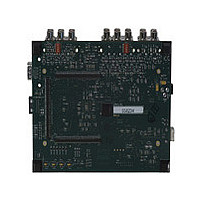
ADDS-BF533-EZLITE Analog Devices Inc, ADDS-BF533-EZLITE Datasheet - Page 19
ADDS-BF533-EZLITE
Manufacturer Part Number
ADDS-BF533-EZLITE
Description
Manufacturer
Analog Devices Inc
Datasheet
1.ADDS-BF533-EZLITE.pdf
(60 pages)
Specifications of ADDS-BF533-EZLITE
Significant Other Parts
ADV7183 Video Decode
Lead Free Status / Rohs Status
Not Compliant


Table 9. Pin Descriptions (Continued)
Pin Name
Port F: GPIO/Parallel Peripheral
Interface Port/SPI/Timers
JTAG Port
SPI Port
Serial Ports
PF0/SPISS
PF1/SPISEL1/TACLK
PF2/SPISEL2
PF3/SPISEL3/PPI_FS3
PF4/SPISEL4/PPI15
PF5/SPISEL5/PPI14
PF6/SPISEL6/PPI13
PF7/SPISEL7/PPI12
PF8/PPI11
PF9/PPI10
PF10/PPI9
PF11/PPI8
PF12/PPI7
PF13/PPI6
PF14/PPI5
PF15/PPI4
TCK
TDO
TDI
TMS
TRST
EMU
MOSI
MISO
SCK
RSCLK0
RFS0
DR0PRI
DR0SEC
TSCLK0
TFS0
DT0PRI
DT0SEC
RSCLK1
Type Function
I/O
I/O
I/O
I/O
I/O
I/O
I/O
I/O
I/O
I/O
I/O
I/O
I/O
I/O
I/O
I/O
I
O
I
I
I
O
I/O
I/O
I/O
I/O
I/O
I
I
I/O
I/O
O
O
I/O
GPIO/SPI Slave Select Input
GPIO/SPI Slave Select Enable 1/Timer Alternate Clock Input
GPIO/SPI Slave Select Enable 2
GPIO/SPI Slave Select Enable 3/PPI Frame Sync 3
GPIO/SPI Slave Select Enable 4/PPI 15
GPIO/SPI Slave Select Enable 5/PPI 14
GPIO/SPI Slave Select Enable 6/PPI 13
GPIO/SPI Slave Select Enable 7/PPI 12
GPIO/PPI 11
GPIO/PPI 10
GPIO/PPI 9
GPIO/PPI 8
GPIO/PPI 7
GPIO/PPI 6
GPIO/PPI 5
GPIO/PPI 4
JTAG Clock
JTAG Serial Data Out
JTAG Serial Data In
JTAG Mode Select
JTAG Reset (This pin should be pulled LOW if JTAG is not used.)
Emulation Output
Master Out Slave In
Master In Slave Out (This pin should be pulled HIGH through a 4.7 kΩ resistor if booting via the
SPI port.)
SPI Clock
SPORT0 Receive Serial Clock
SPORT0 Receive Frame Sync
SPORT0 Receive Data Primary
SPORT0 Receive Data Secondary
SPORT0 Transmit Serial Clock
SPORT0 Transmit Frame Sync
SPORT0 Transmit Data Primary
SPORT0 Transmit Data Secondary
SPORT1 Receive Serial Clock
Rev. E | Page 19 of 60 | July 2007
ADSP-BF531/ADSP-BF532/ADSP-BF533
Driver
Type
C
C
C
C
C
C
C
C
C
C
C
C
C
C
C
C
C
C
C
C
D
D
C
D
C
C
C
D
1