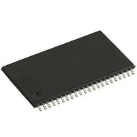
AS4C8M16S-7TCN ALLIANCE MEMORY, AS4C8M16S-7TCN Datasheet - Page 10

AS4C8M16S-7TCN
Manufacturer Part Number
AS4C8M16S-7TCN
Description
DRAM 128M SDRAM 8M X 16 143MHz
Manufacturer
ALLIANCE MEMORY
Datasheet
1.AS4C8M16S-7TCN.pdf
(52 pages)
Specifications of AS4C8M16S-7TCN
Data Bus Width
16 bit
Organization
8 M x 16
Package / Case
TSOP II-54
Memory Size
128 Mbit
Maximum Clock Frequency
143 MHz
Access Time
5.4 ns, 6 ns
Supply Voltage (max)
3.6 V
Supply Voltage (min)
3 V
Maximum Operating Current
130 mA
Maximum Operating Temperature
+ 70 C
Minimum Operating Temperature
0 C
Mounting Style
SMD/SMT
Lead Free Status / Rohs Status
Details
Available stocks
Company
Part Number
Manufacturer
Quantity
Price
precharge function should be issued m cycles after the clock edge in which the last data-in element is
registered, where m equals t
must be used to mask input data, starting with the clock edge following the last data-in element and
ending with the clock edge on which the BankPrecharge/PrechargeAll command is entered (refer to the
following figure).
FEBRUARY 2011
CLK
COMMAND
DQ
t
t
CLK
COMMAND
CAS# latency=2
CAS# latency=3
CK2,
CK3,
issued one cycle after the clock edge in which the last data-in element is registered. In order to avoid
data contention, input data must be removed from the DQs at least one clock cycle before the first
read data appears on the outputs (refer to the following figure). Once the Read command is
registered, the data inputs will be ignored and writes will not be executed.
DQ
DQ
Figure 12. Write Interrupted by a Read
The Read command that interrupts a write burst without auto precharge function should be
The BankPrecharge/PrechargeAll command that interrupts a write burst without the auto
Figure 11. Write Interrupted by a Write
T0
T0
NOP
NOP
WRITE A
WRITE A
T1
DIN A
T1
WR
DIN A
DIN A
/t
CK
0
0
0
rounded up to the next whole number. In addition, the DQM signals
WRITE B
READ B
T2
DIN B
T2
don’t care
don’t care
0
T3
DIN B
T3
NOP
don’t care
NOP
1
10
T4
T4
DOUT B
DIN B
NOP
NOP
(Burst Length = 4, CAS# Latency = 2, 3)
2
0
T5
T5
DOUT B
DOUT B
DIN B
NOP
NOP
Input data must be removed from the DQ
at least one clock cycle before the Read
data appears on the outputs to avoid data
contention
3
(Burst Length = 4)
1
0
T6
T6
DOUT B
DOUT B
NOP
NOP
2
1
DOUT B
T7
T7
DOUT B
NOP
NOP
3
2
T8
T8
DOUT B
NOP
NOP
AS4C8M16S
3


