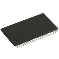
AS4C8M16S-7TCN ALLIANCE MEMORY, AS4C8M16S-7TCN Datasheet - Page 20

AS4C8M16S-7TCN
Manufacturer Part Number
AS4C8M16S-7TCN
Description
DRAM 128M SDRAM 8M X 16 143MHz
Manufacturer
ALLIANCE MEMORY
Datasheet
1.AS4C8M16S-7TCN.pdf
(52 pages)
Specifications of AS4C8M16S-7TCN
Data Bus Width
16 bit
Organization
8 M x 16
Package / Case
TSOP II-54
Memory Size
128 Mbit
Maximum Clock Frequency
143 MHz
Access Time
5.4 ns, 6 ns
Supply Voltage (max)
3.6 V
Supply Voltage (min)
3 V
Maximum Operating Current
130 mA
Maximum Operating Temperature
+ 70 C
Minimum Operating Temperature
0 C
Mounting Style
SMD/SMT
Lead Free Status / Rohs Status
Details
Available stocks
Company
Part Number
Manufacturer
Quantity
Price
Table 17. LVTTL Interface
7. Transition times are measured between V
8. t
9. If clock rising time is longer than 1 ns, (t
10. Assumed input rise and fall time t
11. Power up Sequence
Transition Time (Rise and Fall) of Input Signals
Output
fixed slope (1 ns).
levels.
If t
should be added to the parameter.
FEBRUARY 2011
HZ
Power up must be performed in the following sequence.
1) Power must be applied to V
2) Start clock and maintain stable condition for minimum 200 µs, then bring CKE= “H” and, it is
3) All banks must be precharged.
4) Mode Register Set command must be asserted to initialize the Mode register.
5) A minimum of 2 Auto-Refresh dummy cycles must be required to stabilize the internal circuitry of the
Figure 18.1 LVTTL D.C. Test Load (A)
R
defines the time in which the outputs achieve the open circuit condition and are not at reference
* The Auto Refresh command can be issue before or after Mode Register Set command
signals are held "NOP" state.
recommended that DQM is held "HIGH" (V
device.
Reference Level of Output Signals
or t
Reference Level of Input Signals
F
is longer than 1 ns, transient time compensation should be considered, i.e., [(tr + tf)/2 - 1] ns
Input Signal Levels
30pF
Output Load
1.2kΩ
3.3V
870Ω
DD
T
(t
and V
R
& t
R
F
/ 2 -0.5) ns should be added to the parameter.
) = 1 ns
DDQ
IH
Output
and V
(simultaneously) when CKE= “L”, DQM= “H” and all input
DD
levels) to ensure DQ output is in high impedance.
20
Figure 18.2 LVTTL A.C. Test Load (B)
IL
Reference to the Under Output Load (B)
. Transition (rise and fall) of input signals are in a
Z0=
50 Ω
1.4V / 1.4V
2.4V / 0.4V
1.4V
1ns
30pF
50 Ω
1.4V
AS4C8M16S


