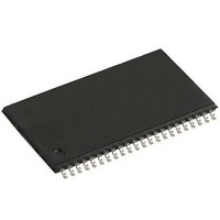
AS4C8M16S-7TCN ALLIANCE MEMORY, AS4C8M16S-7TCN Datasheet - Page 11

AS4C8M16S-7TCN
Manufacturer Part Number
AS4C8M16S-7TCN
Description
DRAM 128M SDRAM 8M X 16 143MHz
Manufacturer
ALLIANCE MEMORY
Datasheet
1.AS4C8M16S-7TCN.pdf
(52 pages)
Specifications of AS4C8M16S-7TCN
Data Bus Width
16 bit
Organization
8 M x 16
Package / Case
TSOP II-54
Memory Size
128 Mbit
Maximum Clock Frequency
143 MHz
Access Time
5.4 ns, 6 ns
Supply Voltage (max)
3.6 V
Supply Voltage (min)
3 V
Maximum Operating Current
130 mA
Maximum Operating Temperature
+ 70 C
Minimum Operating Temperature
0 C
Mounting Style
SMD/SMT
Lead Free Status / Rohs Status
Details
Available stocks
Company
Part Number
Manufacturer
Quantity
Price
7
8
FEBRUARY 2011
Write and AutoPrecharge command (RAS# = "H", CAS# = "L", WE# = "L", BAs = Bank, A10 = "H",
A0-A8 = Column Address)
the write operation. Once this command is given, any subsequent command can not occur within a
time delay of {(burst length -1) + t
performed in this command and the auto precharge function is ignored.
Mode Register Set command programs the values of CAS# latency, Addressing Mode and Burst
Length in the Mode register to make SDRAM useful for a variety of different applications. The default
values of the Mode Register after power-up are undefined; therefore this command must be issued
at the power-up sequence. The state of pins A0~A9 and A11 in the same cycle is the data written to
the mode register. Two clock cycles are required to complete the write in the mode register (refer to
the following figure). The contents of the mode register can be changed using the same command
and the clock cycle requirements during operation as long as all banks are in the idle state.
Note: The DQMs can remain low in this example if the length of the write burst is 1 or 2.
CLK
DQM
COMMAND
DQ
COMMAND
ADDRESS
DQ
CLK
Mode Register Set command (RAS# = "L", CAS# = "L", WE# = "L", A0-A11 = Register Data)
The Write and AutoPrecharge command performs the precharge operation automatically after
The mode register stores the data for controlling the various operating modes of SDRAM. The
Figure 14. Burst Write with Auto-Precharge
t
DAL
=t
Activate
WRITE
Bank A
T0
T0
COL n
BANK
WR
DIN
N
+t
RP
T1
NOP
NOP
T1
DIN
N+1
Figure 13. Write to Precharge
tWR
T2
NOP
NOP
T2
WR
Auto Precharge
BANK(S)
+ t
Precharge
T3
DIN A
Write A
T3
RP
0
(min.)}. At full-page burst, only the write operation is
T4
11
NOP
DIN A
NOP
T4
1
tRP
T5
NOP
NOP
T5
t
DAL
T6
Activate
Begin AutoPrecharge
Bank can be reactivated at
completion of t
NOP
Don’t Care
ROW
T6
(Burst Length = 2)
T7
NOP
NOP
T7
DAL
T8
NOP
AS4C8M16S
Activate
T9
Bank A


