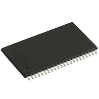
AS4C8M16S-7TCN ALLIANCE MEMORY, AS4C8M16S-7TCN Datasheet - Page 7

AS4C8M16S-7TCN
Manufacturer Part Number
AS4C8M16S-7TCN
Description
DRAM 128M SDRAM 8M X 16 143MHz
Manufacturer
ALLIANCE MEMORY
Datasheet
1.AS4C8M16S-7TCN.pdf
(52 pages)
Specifications of AS4C8M16S-7TCN
Data Bus Width
16 bit
Organization
8 M x 16
Package / Case
TSOP II-54
Memory Size
128 Mbit
Maximum Clock Frequency
143 MHz
Access Time
5.4 ns, 6 ns
Supply Voltage (max)
3.6 V
Supply Voltage (min)
3 V
Maximum Operating Current
130 mA
Maximum Operating Temperature
+ 70 C
Minimum Operating Temperature
0 C
Mounting Style
SMD/SMT
Lead Free Status / Rohs Status
Details
Available stocks
Company
Part Number
Manufacturer
Quantity
Price
FEBRUARY 2011
(i.e. DQM latency is two clocks for output buffers). A read burst without the auto precharge function
may be interrupted by a subsequent Read or Write command to the same bank or the other active
bank before the end of the burst length. It may be interrupted by a BankPrecharge/ PrechargeAll
command to the same bank too. The interrupt coming from the Read command can occur on any
clock cycle following a previous Read command (refer to the following figure).
from a Write command. The DQMs must be asserted (HIGH) at least two clocks prior to the Write
command to suppress data-out on the DQ pins. To guarantee the DQ pins against I/O contention, a
single cycle with high-impedance on the DQ pins must occur between the last read data and the
Write command (refer to the following three figures). If the data output of the burst read occurs at the
second clock of the burst write, the DQMs must be asserted (HIGH) at least one clock prior to the
Write command to avoid internal bus contention.
t
t
t
CK2,
CAS# latency=2
CAS# latency=3
CLK
COMMAND
t
CK2,
CK3,
CLK
COMMAND
CAS# latency=2
CAS# latency=3
CK3,
Figure 5. Read Interrupted by a Read
The read data appears on the DQs subject to the values on the DQM inputs two clocks earlier
The DQM inputs are used to avoid I/O contention on the DQ pins when the interrupt comes
DQ
DQ
DQ
DQ
Figure 4. Burst Read Operation
T0
READ A
READ A READ B
T0
T1
NOP
T1
DOUT A
T2
NOP
DOUT A
T2
NOP
0
0
DOUT A
DOUT A
T3
DOUT A
NOP
DOUT B
T3
NOP
(Burst Length = 4, CAS# Latency = 2, 3)
1
0
(Burst Length = 4, CAS# Latency = 2, 3)
0
DOUT A
DOUT A
0
T4
7
DOUT B
DOUT B
NOP
T4
NOP
2
1
1
0
DOUT A
DOUT A
T5
DOUT B
DOUT B
T5
NOP
NOP
3
2
2
1
DOUT A
T6
DOUT B
DOUT B
T6
NOP
NOP
3
3
2
DOUT B
T7
T7
NOP
NOP
3
AS4C8M16S
T8
NOP
T8
NOP


