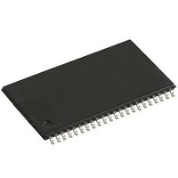
AS4C8M16S-7TCN ALLIANCE MEMORY, AS4C8M16S-7TCN Datasheet - Page 50

AS4C8M16S-7TCN
Manufacturer Part Number
AS4C8M16S-7TCN
Description
DRAM 128M SDRAM 8M X 16 143MHz
Manufacturer
ALLIANCE MEMORY
Datasheet
1.AS4C8M16S-7TCN.pdf
(52 pages)
Specifications of AS4C8M16S-7TCN
Data Bus Width
16 bit
Organization
8 M x 16
Package / Case
TSOP II-54
Memory Size
128 Mbit
Maximum Clock Frequency
143 MHz
Access Time
5.4 ns, 6 ns
Supply Voltage (max)
3.6 V
Supply Voltage (min)
3 V
Maximum Operating Current
130 mA
Maximum Operating Temperature
+ 70 C
Minimum Operating Temperature
0 C
Mounting Style
SMD/SMT
Lead Free Status / Rohs Status
Details
Available stocks
Company
Part Number
Manufacturer
Quantity
Price
Figure 41. Full Page Random Column Write
Figure 42. Precharge Termination of a Burst
A0-A9,
A11
BA0,1
CKE
WE#
DQM
CLK
RAS#
CAS#
CLK
CKE
CS#
RAS#
CAS#
WE#
BA0,1
A10
DQ
A0-A9,
A11
DQM
FEBRUARY 2011
Activate
Cammand
Bank A
High
Hi-Z
RAx
RAx
T0
T0 T1
Activate
Cammand
Bank A
(Burst Length=4, 8 or Full Page, CAS# Latency=3)
RAx
RAx
RAx
t
RRD
Write
Command
Bank A
T2
Activate
Command
Bank B
DAx0
CAx
RBx
RBx
T3 T4 T5 T6 T7 T8 T9 T10
Precharge Termination
of a Write Burst
Write Data are masked
DAx1
Write
Command
Bank A
CAx
DAx0
t
RCD
t
WR
DAx1
Write
Command
Bank B
Precharge
Command
Bank A
DBx0 DAy0 DAy1
CBx
t
RP
Write
Command
Bank A
CAy
Activate
Command
Bank A
Write
Command
Bank B
RAy
RAy
DBy0
CBy
DBy1
50
Write
Command
Bank A
DAz0 DAz1 DAz2 DBz0 DBz1 DBz2
CAz
(Burst Length=Full Page)
T11 T12 T13 T14 T15 T16 T17 T18 T19 T20 T21 T22
Read
Command
Bank A
CAy
Write
Command
Bank B
CBz
Precharge
Command
Bank A
Ay0
t
RP
Ay1 Ay2
Write Data
are masked
t
WR
Precharge
Command Bank B
(Precharge Temination)
Activate
Command
Bank A
RAz
RAz
Don’t Care
t
RP
Precharge Termination
of a Read Burst
AS4C8M16S
Activate
Command
Bank B
RBw
RBw


