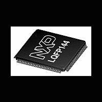
LPC2926_27_29 NXP Semiconductors, LPC2926_27_29 Datasheet - Page 11

LPC2926_27_29
Manufacturer Part Number
LPC2926_27_29
Description
The LPC2926/2927/2929 combine an ARM968E-S CPU core with two integrated TCMblocks operating at frequencies of up to 125 MHz, Full-speed USB 2
Manufacturer
NXP Semiconductors
Datasheet
1.LPC2926_27_29.pdf
(95 pages)
- Current page: 11 of 95
- Download datasheet (2Mb)
NXP Semiconductors
Table 3.
[1]
[2]
[3]
[4]
6. Functional description
LPC2926_27_29
Product data sheet
Pin name
P0[19]/IN2[3]/
PMAT2[1]/A15
P3[4]/MAT3[2]/
PMAT2[4]/TXDC1
P3[5]/MAT3[3]/
PMAT2[5]/RXDC1
P2[18]/SCS2[1]/
PCAP1[1]/D16
P2[19]/SCS2[0]/
PCAP1[2]/D17
P0[20]/IN2[4]/
PMAT2[2]/A16
P0[21]/IN2[5]/
PMAT2[3]/A17
P0[22]/IN2[6]/
PMAT2[4]/A18
V
P0[23]/IN2[7]/
PMAT2[5]/A19
P2[20]/
PCAP2[0]/D18
TDI
SS(IO)
Bidirectional pad; analog port; plain input; 3-state output; slew rate control; 5 V tolerant; TTL with hysteresis; programmable
pull-up/pull-down/repeater.
USB pad.
Analog pad; analog I/O.
Analog I/O pad.
LQFP144 pin assignment
6.1 Architectural overview
Pin
133
134
135
136
137
138
139
140
141
142
143
144
The LPC2926/2927/2929 consists of:
•
•
•
•
•
[4]
[1]
[1]
[1]
[1]
[4]
[4]
[4]
[4]
[1]
[1]
An ARM968E-S processor with real-time emulation support
An AMBA multi-layer Advanced High-performance Bus (AHB) for interfacing to the
on-chip memory controllers
Two DTL buses (an universal NXP interface) for interfacing to the interrupt controller
and the Power, Clock and Reset Control cluster (also called subsystem).
Three ARM Peripheral Buses (APB - a compatible superset of ARM's AMBA
advanced peripheral bus) for connection to on-chip peripherals clustered in
subsystems.
One ARM Peripheral Bus for event router and system control.
Description
Function 0
(default)
GPIO0, pin 19
GPIO3, pin 4
GPIO3, pin 5
GPIO2, pin 18
GPIO2, pin 19
GPIO0, pin 20
GPIO0, pin 21
GPIO0, pin 22
ground for I/O
GPIO0, pin 23
GPIO2, pin 20
IEEE 1149.1 data in, pulled up internally
…continued
All information provided in this document is subject to legal disclaimers.
Rev. 5 — 28 September 2010
Function 1
ADC2 IN3
TIMER3 MAT2
TIMER3 MAT3
ADC2 IN4
ADC2 IN5
ADC2 IN6
ADC2 IN7
SPI2 SDO
SPI2 SCS1
SPI2 SCS0
ARM9 microcontroller with CAN, LIN, and USB
LPC2926/2927/2929
PWM2 MAT4
PWM2 MAT5
Function 2
PWM2 MAT1
PWM1 CAP1
PWM1 CAP2
PWM2 MAT2
PWM2 MAT3
PWM2 MAT4
PWM2 MAT5
PWM2 CAP0
© NXP B.V. 2010. All rights reserved.
Function 3
EXTBUS A15
CAN1 TXD
CAN1 RXD
EXTBUS D16
EXTBUS D17
EXTBUS A16
EXTBUS A17
EXTBUS A18
EXTBUS A19
EXTBUS D18
11 of 95
Related parts for LPC2926_27_29
Image
Part Number
Description
Manufacturer
Datasheet
Request
R
Part Number:
Description:
Lpc2926/2927/2929 Arm9 Microcontroller With Can, Lin, And Usb
Manufacturer:
NXP Semiconductors
Datasheet:
Part Number:
Description:
NXP Semiconductors designed the LPC2420/2460 microcontroller around a 16-bit/32-bitARM7TDMI-S CPU core with real-time debug interfaces that include both JTAG andembedded trace
Manufacturer:
NXP Semiconductors
Datasheet:

Part Number:
Description:
NXP Semiconductors designed the LPC2458 microcontroller around a 16-bit/32-bitARM7TDMI-S CPU core with real-time debug interfaces that include both JTAG andembedded trace
Manufacturer:
NXP Semiconductors
Datasheet:
Part Number:
Description:
NXP Semiconductors designed the LPC2468 microcontroller around a 16-bit/32-bitARM7TDMI-S CPU core with real-time debug interfaces that include both JTAG andembedded trace
Manufacturer:
NXP Semiconductors
Datasheet:
Part Number:
Description:
NXP Semiconductors designed the LPC2470 microcontroller, powered by theARM7TDMI-S core, to be a highly integrated microcontroller for a wide range ofapplications that require advanced communications and high quality graphic displays
Manufacturer:
NXP Semiconductors
Datasheet:
Part Number:
Description:
NXP Semiconductors designed the LPC2478 microcontroller, powered by theARM7TDMI-S core, to be a highly integrated microcontroller for a wide range ofapplications that require advanced communications and high quality graphic displays
Manufacturer:
NXP Semiconductors
Datasheet:
Part Number:
Description:
The Philips Semiconductors XA (eXtended Architecture) family of 16-bit single-chip microcontrollers is powerful enough to easily handle the requirements of high performance embedded applications, yet inexpensive enough to compete in the market for hi
Manufacturer:
NXP Semiconductors
Datasheet:
Part Number:
Description:
The XA-S3 device is a member of Philips Semiconductors? XA(eXtended Architecture) family of high performance 16-bitsingle-chip microcontrollers
Manufacturer:
NXP Semiconductors
Datasheet:

Part Number:
Description:
The NXP BlueStreak LH75401/LH75411 family consists of two low-cost 16/32-bit System-on-Chip (SoC) devices
Manufacturer:
NXP Semiconductors
Datasheet:

Part Number:
Description:
The NXP LPC3130/3131 combine an 180 MHz ARM926EJ-S CPU core, high-speed USB2
Manufacturer:
NXP Semiconductors
Datasheet:

Part Number:
Description:
The NXP LPC3141 combine a 270 MHz ARM926EJ-S CPU core, High-speed USB 2
Manufacturer:
NXP Semiconductors

Part Number:
Description:
The NXP LPC3143 combine a 270 MHz ARM926EJ-S CPU core, High-speed USB 2
Manufacturer:
NXP Semiconductors

Part Number:
Description:
The NXP LPC3152 combines an 180 MHz ARM926EJ-S CPU core, High-speed USB 2
Manufacturer:
NXP Semiconductors

Part Number:
Description:
The NXP LPC3154 combines an 180 MHz ARM926EJ-S CPU core, High-speed USB 2
Manufacturer:
NXP Semiconductors


