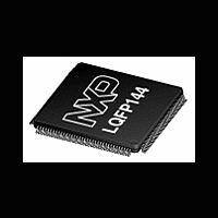
LPC2926_27_29 NXP Semiconductors, LPC2926_27_29 Datasheet - Page 20

LPC2926_27_29
Manufacturer Part Number
LPC2926_27_29
Description
The LPC2926/2927/2929 combine an ARM968E-S CPU core with two integrated TCMblocks operating at frequencies of up to 125 MHz, Full-speed USB 2
Manufacturer
NXP Semiconductors
Datasheet
1.LPC2926_27_29.pdf
(95 pages)
- Current page: 20 of 95
- Download datasheet (2Mb)
NXP Semiconductors
LPC2926_27_29
Product data sheet
6.8.1 Functional description
6.8 Flash memory controller
The flash memory has a 128-bit wide data interface and the flash controller offers two
128-bit buffer lines to improve system performance. The flash has to be programmed
initially via JTAG. In-system programming must be supported by the bootloader. Flash
memory contents can be protected by disabling JTAG access. Suspension of burning or
erasing is not supported.
The Flash Memory Controller (FMC) interfaces to the embedded flash memory for two
tasks:
The key features are:
After reset, flash initialization is started, which takes t
initialization, flash access is not possible and AHB transfers to flash are stalled, blocking
the AHB bus.
During flash initialization, the index sector is read to identify the status of the JTAG access
protection and sector security. If JTAG access protection is active, the flash is not
accessible via JTAG. In this case, ARM debug facilities are disabled and flash memory
contents cannot be read. If sector security is active, only the unsecured sections can be
read.
Flash can be read synchronously or asynchronously to the system clock. In synchronous
operation, the flash goes into standby after returning the read data. Started reads cannot
be stopped, and speculative reading and dual buffering are therefore not supported.
With asynchronous reading, transfer of the address to the flash and of read data from the
flash is done asynchronously, giving the fastest possible response time. Started reads can
be stopped, so speculative reading and dual buffering are supported.
Buffering is offered because the flash has a 128-bit wide data interface while the AHB
interface has only 32 bits. With buffering a buffer line holds the complete 128-bit flash
word, from which four words can be read. Without buffering every AHB data port read
starts a flash read. A flash read is a slow process compared to the minimum AHB cycle
time, so with buffering the average read time is reduced. This can improve system
performance.
With single buffering, the most recently read flash word remains available until the next
flash read. When an AHB data-port read transfer requires data from the same flash word
as the previous read transfer, no new flash read is done and the read data is given without
wait cycles.
•
•
•
•
•
•
Memory data transfer
Memory configuration via triggering, programming, and erasing
Programming by CPU via AHB
Programming by external programmer via JTAG
JTAG access protection
Burn-finished and erase-finished interrupt
All information provided in this document is subject to legal disclaimers.
Rev. 5 — 28 September 2010
ARM9 microcontroller with CAN, LIN, and USB
LPC2926/2927/2929
init
time (see
Section
© NXP B.V. 2010. All rights reserved.
9). During this
20 of 95
Related parts for LPC2926_27_29
Image
Part Number
Description
Manufacturer
Datasheet
Request
R
Part Number:
Description:
Lpc2926/2927/2929 Arm9 Microcontroller With Can, Lin, And Usb
Manufacturer:
NXP Semiconductors
Datasheet:
Part Number:
Description:
NXP Semiconductors designed the LPC2420/2460 microcontroller around a 16-bit/32-bitARM7TDMI-S CPU core with real-time debug interfaces that include both JTAG andembedded trace
Manufacturer:
NXP Semiconductors
Datasheet:

Part Number:
Description:
NXP Semiconductors designed the LPC2458 microcontroller around a 16-bit/32-bitARM7TDMI-S CPU core with real-time debug interfaces that include both JTAG andembedded trace
Manufacturer:
NXP Semiconductors
Datasheet:
Part Number:
Description:
NXP Semiconductors designed the LPC2468 microcontroller around a 16-bit/32-bitARM7TDMI-S CPU core with real-time debug interfaces that include both JTAG andembedded trace
Manufacturer:
NXP Semiconductors
Datasheet:
Part Number:
Description:
NXP Semiconductors designed the LPC2470 microcontroller, powered by theARM7TDMI-S core, to be a highly integrated microcontroller for a wide range ofapplications that require advanced communications and high quality graphic displays
Manufacturer:
NXP Semiconductors
Datasheet:
Part Number:
Description:
NXP Semiconductors designed the LPC2478 microcontroller, powered by theARM7TDMI-S core, to be a highly integrated microcontroller for a wide range ofapplications that require advanced communications and high quality graphic displays
Manufacturer:
NXP Semiconductors
Datasheet:
Part Number:
Description:
The Philips Semiconductors XA (eXtended Architecture) family of 16-bit single-chip microcontrollers is powerful enough to easily handle the requirements of high performance embedded applications, yet inexpensive enough to compete in the market for hi
Manufacturer:
NXP Semiconductors
Datasheet:
Part Number:
Description:
The XA-S3 device is a member of Philips Semiconductors? XA(eXtended Architecture) family of high performance 16-bitsingle-chip microcontrollers
Manufacturer:
NXP Semiconductors
Datasheet:

Part Number:
Description:
The NXP BlueStreak LH75401/LH75411 family consists of two low-cost 16/32-bit System-on-Chip (SoC) devices
Manufacturer:
NXP Semiconductors
Datasheet:

Part Number:
Description:
The NXP LPC3130/3131 combine an 180 MHz ARM926EJ-S CPU core, high-speed USB2
Manufacturer:
NXP Semiconductors
Datasheet:

Part Number:
Description:
The NXP LPC3141 combine a 270 MHz ARM926EJ-S CPU core, High-speed USB 2
Manufacturer:
NXP Semiconductors

Part Number:
Description:
The NXP LPC3143 combine a 270 MHz ARM926EJ-S CPU core, High-speed USB 2
Manufacturer:
NXP Semiconductors

Part Number:
Description:
The NXP LPC3152 combines an 180 MHz ARM926EJ-S CPU core, High-speed USB 2
Manufacturer:
NXP Semiconductors

Part Number:
Description:
The NXP LPC3154 combines an 180 MHz ARM926EJ-S CPU core, High-speed USB 2
Manufacturer:
NXP Semiconductors


