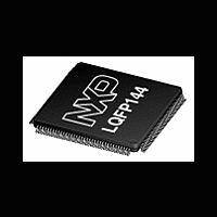
LPC2926_27_29 NXP Semiconductors, LPC2926_27_29 Datasheet - Page 37

LPC2926_27_29
Manufacturer Part Number
LPC2926_27_29
Description
The LPC2926/2927/2929 combine an ARM968E-S CPU core with two integrated TCMblocks operating at frequencies of up to 125 MHz, Full-speed USB 2
Manufacturer
NXP Semiconductors
Datasheet
1.LPC2926_27_29.pdf
(95 pages)
- Current page: 37 of 95
- Download datasheet (2Mb)
NXP Semiconductors
LPC2926_27_29
Product data sheet
6.14.1.2 Pin description
6.14.2.1 Pin description
6.14.2 LIN
6.14.3 I
The two CAN controllers in the LPC2926/2927/2929 have the pins listed below. The CAN
pins are combined with other functions on the port pins of the LPC2926/2927/2929.
Table 20
Table 20.
The LPC2926/2927/2929 contain two LIN 2.0 master controllers. These can be used as
dedicated LIN 2.0 master controllers with additional support for sync break generation and
with hardware implementation of the LIN protocol according to spec 2.0.
Remark: Both LIN channels can be also configured as UART channels.
The key features are:
The two LIN 2.0 master controllers in the LPC2926/2927/2929 have the pins listed below.
The LIN pins are combined with other functions on the port pins of the
LPC2926/2927/2929.
subsection 3.43, LIN master controller.
Table 21.
The LPC2926/2927/2929 each contain two I
The I
(SCL) and a Serial DAta line (SDA). Each device is recognized by a unique address and
can operate as either a receiver-only device (e.g., an LCD driver) or as a transmitter with
the capability to both receive and send information (such as memory). Transmitters and/or
Symbol
CANx TXD
CANx RXD
Symbol
LIN0/1 TXD
LIN0/1 RXD
2
•
•
•
•
•
•
•
•
•
•
C-bus serial I/O controllers
Complete LIN 2.0 message handling and transfer
One interrupt per LIN message
Slave response time-out detection
Programmable sync-break length
Automatic sync-field and sync-break generation
Programmable inter-byte space
Hardware or software parity generation
Automatic checksum generation
Fault confinement
Fractional baud rate generator
2
C-bus is bidirectional for inter-IC control using only two wires: a Serial CLock line
shows the CAN pins (x runs from 0 to 1).
CAN pins
LIN controller pins
Pin name
TXDC0/1
RXDC0/1
Pin name
TXDL0/1
RXDL0/1
All information provided in this document is subject to legal disclaimers.
Rev. 5 — 28 September 2010
Table 21
Direction
OUT
IN
Direction
OUT
IN
shows the LIN pins. For more information see
ARM9 microcontroller with CAN, LIN, and USB
Description
CAN channel x transmit data output
CAN channel x receive data input
Description
LIN channel 0/1 transmit data output
LIN channel 0/1 receive data input
2
C-bus controllers.
LPC2926/2927/2929
© NXP B.V. 2010. All rights reserved.
Ref. 1
37 of 95
Related parts for LPC2926_27_29
Image
Part Number
Description
Manufacturer
Datasheet
Request
R
Part Number:
Description:
Lpc2926/2927/2929 Arm9 Microcontroller With Can, Lin, And Usb
Manufacturer:
NXP Semiconductors
Datasheet:
Part Number:
Description:
NXP Semiconductors designed the LPC2420/2460 microcontroller around a 16-bit/32-bitARM7TDMI-S CPU core with real-time debug interfaces that include both JTAG andembedded trace
Manufacturer:
NXP Semiconductors
Datasheet:

Part Number:
Description:
NXP Semiconductors designed the LPC2458 microcontroller around a 16-bit/32-bitARM7TDMI-S CPU core with real-time debug interfaces that include both JTAG andembedded trace
Manufacturer:
NXP Semiconductors
Datasheet:
Part Number:
Description:
NXP Semiconductors designed the LPC2468 microcontroller around a 16-bit/32-bitARM7TDMI-S CPU core with real-time debug interfaces that include both JTAG andembedded trace
Manufacturer:
NXP Semiconductors
Datasheet:
Part Number:
Description:
NXP Semiconductors designed the LPC2470 microcontroller, powered by theARM7TDMI-S core, to be a highly integrated microcontroller for a wide range ofapplications that require advanced communications and high quality graphic displays
Manufacturer:
NXP Semiconductors
Datasheet:
Part Number:
Description:
NXP Semiconductors designed the LPC2478 microcontroller, powered by theARM7TDMI-S core, to be a highly integrated microcontroller for a wide range ofapplications that require advanced communications and high quality graphic displays
Manufacturer:
NXP Semiconductors
Datasheet:
Part Number:
Description:
The Philips Semiconductors XA (eXtended Architecture) family of 16-bit single-chip microcontrollers is powerful enough to easily handle the requirements of high performance embedded applications, yet inexpensive enough to compete in the market for hi
Manufacturer:
NXP Semiconductors
Datasheet:
Part Number:
Description:
The XA-S3 device is a member of Philips Semiconductors? XA(eXtended Architecture) family of high performance 16-bitsingle-chip microcontrollers
Manufacturer:
NXP Semiconductors
Datasheet:

Part Number:
Description:
The NXP BlueStreak LH75401/LH75411 family consists of two low-cost 16/32-bit System-on-Chip (SoC) devices
Manufacturer:
NXP Semiconductors
Datasheet:

Part Number:
Description:
The NXP LPC3130/3131 combine an 180 MHz ARM926EJ-S CPU core, high-speed USB2
Manufacturer:
NXP Semiconductors
Datasheet:

Part Number:
Description:
The NXP LPC3141 combine a 270 MHz ARM926EJ-S CPU core, High-speed USB 2
Manufacturer:
NXP Semiconductors

Part Number:
Description:
The NXP LPC3143 combine a 270 MHz ARM926EJ-S CPU core, High-speed USB 2
Manufacturer:
NXP Semiconductors

Part Number:
Description:
The NXP LPC3152 combines an 180 MHz ARM926EJ-S CPU core, High-speed USB 2
Manufacturer:
NXP Semiconductors

Part Number:
Description:
The NXP LPC3154 combines an 180 MHz ARM926EJ-S CPU core, High-speed USB 2
Manufacturer:
NXP Semiconductors


