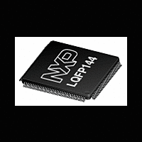
LPC2926_27_29 NXP Semiconductors, LPC2926_27_29 Datasheet - Page 36

LPC2926_27_29
Manufacturer Part Number
LPC2926_27_29
Description
The LPC2926/2927/2929 combine an ARM968E-S CPU core with two integrated TCMblocks operating at frequencies of up to 125 MHz, Full-speed USB 2
Manufacturer
NXP Semiconductors
Datasheet
1.LPC2926_27_29.pdf
(95 pages)
- Current page: 36 of 95
- Download datasheet (2Mb)
NXP Semiconductors
LPC2926_27_29
Product data sheet
6.13.6.3 Clock description
6.14.1.1 Global acceptance filter
6.14.1 CAN gateway
6.14 Networking subsystem
Table 19.
The GPIO modules are clocked by several clocks, all of which are derived from
BASE_SYS_CLK; CLK_SYS_PESS and CLK_SYS_GPIOx (x = 0, 1, 2, 3, 5), see
Section
management. The frequency of all clocks CLK_SYS_GPIOx is identical to
CLK_SYS_PESS since they are derived from the same base clock BASE_SYS_CLK.
Controller Area Network (CAN) is the definition of a high-performance communication
protocol for serial data communication. The two CAN controllers in the
LPC2926/2927/2929 provide a full implementation of the CAN protocol according to the
CAN specification version 2.0B. The gateway concept is fully scalable with the number of
CAN controllers, and always operates together with a separate powerful and flexible
hardware acceptance filter.
The key features are:
The global acceptance filter provides look-up of received identifiers - called acceptance
filtering in CAN terminology - for all the CAN controllers. It includes a CAN ID look-up table
memory, in which software maintains one to five sections of identifiers. The CAN ID
look-up table memory is 2 kB large (512 words, each of 32 bits). It can contain up to 1024
standard frame identifiers or 512 extended frame identifiers or a mixture of both types. It is
also possible to define identifier groups for standard and extended message formats.
Symbol
GPIO0 pin[31:0]
GPIO1 pin[27:0]
GPIO2 pin[27:0]
GPIO3 pin[15:0]
GPIO5 pin[19:18]
•
•
•
•
•
•
•
•
Supports 11-bit as well as 29-bit identifiers
Double receive buffer and triple transmit buffer
Programmable error-warning limit and error counters with read/write access
Arbitration-lost capture and error-code capture with detailed bit position
Single-shot transmission (i.e. no re-transmission)
Listen-only mode (no acknowledge; no active error flags)
Reception of ‘own’ messages (self-reception request)
FullCAN mode for message reception
6.7.2. Note that each GPIO has its own CLK_SYS_GPIOx branch clock for power
GPIO pins
All information provided in this document is subject to legal disclaimers.
Rev. 5 — 28 September 2010
Pin name
P0[31:0]
P1[27:0]
P2[27:0]
P3[15:0]
P5[19:18]
ARM9 microcontroller with CAN, LIN, and USB
Direction
IN/OUT
IN/OUT
IN/OUT
IN/OUT
IN/OUT
LPC2926/2927/2929
Description
GPIO port x pins 31 to 0
GPIO port x pins 27 to 0
GPIO port x pins 27 to 0
GPIO port x pins 15 to 0
GPIO port x pins 19 and 18
© NXP B.V. 2010. All rights reserved.
36 of 95
Related parts for LPC2926_27_29
Image
Part Number
Description
Manufacturer
Datasheet
Request
R
Part Number:
Description:
Lpc2926/2927/2929 Arm9 Microcontroller With Can, Lin, And Usb
Manufacturer:
NXP Semiconductors
Datasheet:
Part Number:
Description:
NXP Semiconductors designed the LPC2420/2460 microcontroller around a 16-bit/32-bitARM7TDMI-S CPU core with real-time debug interfaces that include both JTAG andembedded trace
Manufacturer:
NXP Semiconductors
Datasheet:

Part Number:
Description:
NXP Semiconductors designed the LPC2458 microcontroller around a 16-bit/32-bitARM7TDMI-S CPU core with real-time debug interfaces that include both JTAG andembedded trace
Manufacturer:
NXP Semiconductors
Datasheet:
Part Number:
Description:
NXP Semiconductors designed the LPC2468 microcontroller around a 16-bit/32-bitARM7TDMI-S CPU core with real-time debug interfaces that include both JTAG andembedded trace
Manufacturer:
NXP Semiconductors
Datasheet:
Part Number:
Description:
NXP Semiconductors designed the LPC2470 microcontroller, powered by theARM7TDMI-S core, to be a highly integrated microcontroller for a wide range ofapplications that require advanced communications and high quality graphic displays
Manufacturer:
NXP Semiconductors
Datasheet:
Part Number:
Description:
NXP Semiconductors designed the LPC2478 microcontroller, powered by theARM7TDMI-S core, to be a highly integrated microcontroller for a wide range ofapplications that require advanced communications and high quality graphic displays
Manufacturer:
NXP Semiconductors
Datasheet:
Part Number:
Description:
The Philips Semiconductors XA (eXtended Architecture) family of 16-bit single-chip microcontrollers is powerful enough to easily handle the requirements of high performance embedded applications, yet inexpensive enough to compete in the market for hi
Manufacturer:
NXP Semiconductors
Datasheet:
Part Number:
Description:
The XA-S3 device is a member of Philips Semiconductors? XA(eXtended Architecture) family of high performance 16-bitsingle-chip microcontrollers
Manufacturer:
NXP Semiconductors
Datasheet:

Part Number:
Description:
The NXP BlueStreak LH75401/LH75411 family consists of two low-cost 16/32-bit System-on-Chip (SoC) devices
Manufacturer:
NXP Semiconductors
Datasheet:

Part Number:
Description:
The NXP LPC3130/3131 combine an 180 MHz ARM926EJ-S CPU core, high-speed USB2
Manufacturer:
NXP Semiconductors
Datasheet:

Part Number:
Description:
The NXP LPC3141 combine a 270 MHz ARM926EJ-S CPU core, High-speed USB 2
Manufacturer:
NXP Semiconductors

Part Number:
Description:
The NXP LPC3143 combine a 270 MHz ARM926EJ-S CPU core, High-speed USB 2
Manufacturer:
NXP Semiconductors

Part Number:
Description:
The NXP LPC3152 combines an 180 MHz ARM926EJ-S CPU core, High-speed USB 2
Manufacturer:
NXP Semiconductors

Part Number:
Description:
The NXP LPC3154 combines an 180 MHz ARM926EJ-S CPU core, High-speed USB 2
Manufacturer:
NXP Semiconductors


