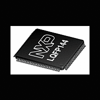
LPC2926_27_29 NXP Semiconductors, LPC2926_27_29 Datasheet - Page 26

LPC2926_27_29
Manufacturer Part Number
LPC2926_27_29
Description
The LPC2926/2927/2929 combine an ARM968E-S CPU core with two integrated TCMblocks operating at frequencies of up to 125 MHz, Full-speed USB 2
Manufacturer
NXP Semiconductors
Datasheet
1.LPC2926_27_29.pdf
(95 pages)
- Current page: 26 of 95
- Download datasheet (2Mb)
NXP Semiconductors
LPC2926_27_29
Product data sheet
6.10.1 DMA support for peripherals
6.10 General Purpose DMA (GPDMA) controller
Usage of the idle/turn-around time (IDCY) is demonstrated In
are added between a read and a write cycle in the same external memory device.
Address pins on the device are shared with other functions. When connecting external
memories, check that the I/O pin is programmed for the correct function. Control of these
settings is handled by the SCU.
The GPDMA controller allows peripheral-to memory, memory-to-peripheral,
peripheral-to-peripheral, and memory-to-memory transactions. Each DMA stream
provides unidirectional serial DMA transfers for a single source and destination. For
example, a bidirectional port requires one stream for transmit and one for receives. The
source and destination areas can each be either a memory region or a peripheral, and
can be accessed through the same AHB master or one area by each master.
The GPDMA controls eight DMA channels with hardware prioritization. The DMA
controller interfaces to the system via two AHB bus masters, each with a full 32-bit data
bus width. DMA operations may be set up for 8-bit, 16-bit, and 32-bit data widths, and can
be either big-endian or little-endian. Incrementing or non-incrementing addressing for
source and destination are supported, as well as programmable DMA burst size. Scatter
or gather DMA is supported through the use of linked lists. This means that the source
and destination areas do not have to occupy contiguous areas of memory.
The GPDMA supports the following peripherals: SPI0/1/2 and UART0/1. The GPDMA can
access both embedded SRAM blocks (16 kB and 32 kB), both TCMs, external static
memory, and flash memory.
Fig 7.
CLK(SYS)
WE
CS
OE
D
A
WSTOEN = 2, WSTWEN = 4, WST1 = 6, WST2 = 4, IDCY = 5
Reading/writing external memory
All information provided in this document is subject to legal disclaimers.
WSTOEN
Rev. 5 — 28 September 2010
WST1
ARM9 microcontroller with CAN, LIN, and USB
IDCY
LPC2926/2927/2929
WSTWEN
Figure
WST2
7. Extra wait states
© NXP B.V. 2010. All rights reserved.
002aae706
26 of 95
Related parts for LPC2926_27_29
Image
Part Number
Description
Manufacturer
Datasheet
Request
R
Part Number:
Description:
Lpc2926/2927/2929 Arm9 Microcontroller With Can, Lin, And Usb
Manufacturer:
NXP Semiconductors
Datasheet:
Part Number:
Description:
NXP Semiconductors designed the LPC2420/2460 microcontroller around a 16-bit/32-bitARM7TDMI-S CPU core with real-time debug interfaces that include both JTAG andembedded trace
Manufacturer:
NXP Semiconductors
Datasheet:

Part Number:
Description:
NXP Semiconductors designed the LPC2458 microcontroller around a 16-bit/32-bitARM7TDMI-S CPU core with real-time debug interfaces that include both JTAG andembedded trace
Manufacturer:
NXP Semiconductors
Datasheet:
Part Number:
Description:
NXP Semiconductors designed the LPC2468 microcontroller around a 16-bit/32-bitARM7TDMI-S CPU core with real-time debug interfaces that include both JTAG andembedded trace
Manufacturer:
NXP Semiconductors
Datasheet:
Part Number:
Description:
NXP Semiconductors designed the LPC2470 microcontroller, powered by theARM7TDMI-S core, to be a highly integrated microcontroller for a wide range ofapplications that require advanced communications and high quality graphic displays
Manufacturer:
NXP Semiconductors
Datasheet:
Part Number:
Description:
NXP Semiconductors designed the LPC2478 microcontroller, powered by theARM7TDMI-S core, to be a highly integrated microcontroller for a wide range ofapplications that require advanced communications and high quality graphic displays
Manufacturer:
NXP Semiconductors
Datasheet:
Part Number:
Description:
The Philips Semiconductors XA (eXtended Architecture) family of 16-bit single-chip microcontrollers is powerful enough to easily handle the requirements of high performance embedded applications, yet inexpensive enough to compete in the market for hi
Manufacturer:
NXP Semiconductors
Datasheet:
Part Number:
Description:
The XA-S3 device is a member of Philips Semiconductors? XA(eXtended Architecture) family of high performance 16-bitsingle-chip microcontrollers
Manufacturer:
NXP Semiconductors
Datasheet:

Part Number:
Description:
The NXP BlueStreak LH75401/LH75411 family consists of two low-cost 16/32-bit System-on-Chip (SoC) devices
Manufacturer:
NXP Semiconductors
Datasheet:

Part Number:
Description:
The NXP LPC3130/3131 combine an 180 MHz ARM926EJ-S CPU core, high-speed USB2
Manufacturer:
NXP Semiconductors
Datasheet:

Part Number:
Description:
The NXP LPC3141 combine a 270 MHz ARM926EJ-S CPU core, High-speed USB 2
Manufacturer:
NXP Semiconductors

Part Number:
Description:
The NXP LPC3143 combine a 270 MHz ARM926EJ-S CPU core, High-speed USB 2
Manufacturer:
NXP Semiconductors

Part Number:
Description:
The NXP LPC3152 combines an 180 MHz ARM926EJ-S CPU core, High-speed USB 2
Manufacturer:
NXP Semiconductors

Part Number:
Description:
The NXP LPC3154 combines an 180 MHz ARM926EJ-S CPU core, High-speed USB 2
Manufacturer:
NXP Semiconductors


