PSD835G2-90UI STMicroelectronics, PSD835G2-90UI Datasheet - Page 14
PSD835G2-90UI
Manufacturer Part Number
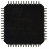
PSD835G2-90UI
Description
IC FLASH 4MBIT 90NS 80TQFP
Manufacturer
STMicroelectronics
Datasheet
1.PSD835G2-90U.pdf
(120 pages)
Specifications of PSD835G2-90UI
Format - Memory
FLASH
Memory Type
FLASH
Memory Size
4M (512K x 8)
Speed
90ns
Interface
Parallel
Voltage - Supply
4.5 V ~ 5.5 V
Operating Temperature
-40°C ~ 85°C
Package / Case
80-TQFP, 80-VQFP
Lead Free Status / RoHS Status
Lead free / RoHS Compliant
Other names
497-2016
Available stocks
Company
Part Number
Manufacturer
Quantity
Price
Company:

Part Number:
PSD835G2-90UI
Manufacturer:
ST
Quantity:
201
Company:
Part Number:
PSD835G2-90UI
Manufacturer:
STMicroelectronics
Quantity:
10 000


Description
Table 1.
14/120
ADIO0-7
ADIO8-
CNTL0
CNTL1
CNTL2
name
Reset
Pin
15
10-12
13-20
3-7-
Pin
Pin description
59
60
40
39
Type
I/O
I/O
I
I
I
I
This is the lower Address/Data port. Connect your MCU address or address/data
bus according to the following rules:
If your MCU has a multiplexed address/data bus where the data is multiplexed
with the lower address bits, connect AD0-AD7 to this port.
If your MCU does not have a multiplexed address/data bus, connect A0-A7 to this
port.
If you are using an 80C51XA in burst mode, connect A4/D0 through A11/D7 to this
port.
ALE or AS latches the address. The PSD drives data out only if the READ signal
is active and one of the PSD functional blocks was selected. The addresses on
this port are passed to the PLDs.
This is the upper Address/Data port. Connect your MCU address or address/data
bus according to the following rules:
If your MCU has a multiplexed address/data bus where the data is multiplexed
with the lower address bits, connect A8-A15 to this port.
If your MCU does not have a multiplexed address/data bus, connect A8-A15 to
this port.
If you are using an 80C251 in page mode, connect AD8-AD15 to this port.
If you are using an 80C51XA in burst mode, connect A12-A19 to this port.
ALE or AS latches the address. The PSD drives data out only if the READ signal
is active and one of the PSD functional blocks was selected. The addresses on
this port are passed to the PLDs.
The following control signals can be connected to this port, based on your MCU:
WR – active low Write Strobe input.
R_W – active high READ/active low WRITE input.
This port is connected to the PLDs. Therefore, these signals can be used in
decode and other logic equations.
The following control signals can be connected to this port, based on your MCU:
RD – active low Read Strobe input.
E – E clock input.
DS – active low Data Strobe input.
PSEN – connect PSEN to this port when it is being used as an active low READ
signal. For example, when the 80C251 outputs more than 16 address bits, PSEN
is actually the READ signal.
This port is connected to the PLDs. Therefore, these signals can be used in
decode and other logic equations.
This port can be used to input the PSEN (Program Select Enable) signal from any
MCU that uses this signal for code exclusively. If your MCU does not output a
Program Select Enable signal, this port can be used as a generic input. This port
is connected to the PLDs as input.
Active low input. Resets I/O ports, PLD macrocells and some of the Configuration
registers and JTAG registers. Must be low at Power-up. Reset also aborts the
Flash programming/erase cycle that is in progress.
Description
PSD835G2
Related parts for PSD835G2-90UI
Image
Part Number
Description
Manufacturer
Datasheet
Request
R

Part Number:
Description:
IC FLASH 4MBIT 90NS 80TQFP
Manufacturer:
STMicroelectronics
Datasheet:
Part Number:
Description:
IC FLASH 4MBIT 70NS 80TQFP
Manufacturer:
STMicroelectronics
Datasheet:
Part Number:
Description:
Configurable Memory System On A Chip For 8-bit Microcontrollers
Manufacturer:
STMicroelectronics
Datasheet:

Part Number:
Description:
Three Phase Rectifier Bridge
Manufacturer:
POWERSEM [Powersem GmbH]
Datasheet:
Part Number:
Description:
STMicroelectronics [RIPPLE-CARRY BINARY COUNTER/DIVIDERS]
Manufacturer:
STMicroelectronics
Datasheet:
Part Number:
Description:
STMicroelectronics [LIQUID-CRYSTAL DISPLAY DRIVERS]
Manufacturer:
STMicroelectronics
Datasheet:

Part Number:
Description:
BOARD EVAL FOR MEMS SENSORS
Manufacturer:
STMicroelectronics
Datasheet:
Part Number:
Description:
NPN TRANSISTOR POWER MODULE
Manufacturer:
STMicroelectronics
Datasheet:
Part Number:
Description:
TURBOSWITCH ULTRA-FAST HIGH VOLTAGE DIODE
Manufacturer:
STMicroelectronics
Datasheet:
Part Number:
Description:
Manufacturer:
STMicroelectronics
Datasheet:
Part Number:
Description:
DIODE / SCR MODULE
Manufacturer:
STMicroelectronics
Datasheet:
Part Number:
Description:
DIODE / SCR MODULE
Manufacturer:
STMicroelectronics
Datasheet: