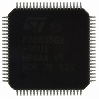
PSD835G2-90UI STMicroelectronics, PSD835G2-90UI Datasheet - Page 34

PSD835G2-90UI
Manufacturer Part Number
PSD835G2-90UI
Description
IC FLASH 4MBIT 90NS 80TQFP
Manufacturer
STMicroelectronics
Datasheet
1.PSD835G2-90U.pdf
(120 pages)
Specifications of PSD835G2-90UI
Format - Memory
FLASH
Memory Type
FLASH
Memory Size
4M (512K x 8)
Speed
90ns
Interface
Parallel
Voltage - Supply
4.5 V ~ 5.5 V
Operating Temperature
-40°C ~ 85°C
Package / Case
80-TQFP, 80-VQFP
Lead Free Status / RoHS Status
Lead free / RoHS Compliant
Other names
497-2016
Available stocks
Company
Part Number
Manufacturer
Quantity
Price
Company:
Part Number:
PSD835G2-90UI
Manufacturer:
ST
Quantity:
201
Company:
Part Number:
PSD835G2-90UI
Manufacturer:
STMicroelectronics
Quantity:
10 000
Detailed operation
Figure 5.
6.5
6.6
34/120
Figure 4.
Selecting the upper or lower block in a primary Flash memory sector
Ready/Busy (PE4)
This signal can be used to output the Ready/Busy status of the PSD. The output on
Ready/Busy (PE4) is a ’0’ (Busy) when Flash memory blocks are being written to, or when
the Flash memory block is being erased. The output is a '1' (Ready) when no WRITE or
Erase cycle is in progress.
Memory operation
The primary Flash memory and secondary Flash memory are addressed through the MCU
Bus Interface. The MCU can access these memories in one of two ways:
●
●
Typically, the MCU can read Flash memory using READ operations, just as it would read a
ROM device. However, Flash memory can only be altered using specific Erase and Program
instructions. For example, the MCU cannot write a single byte directly to Flash memory as it
would write a byte to RAM. To program a byte into Flash memory, the MCU must execute a
Program instruction, then test the status of the Program cycle. This status test is achieved
by a READ operation or polling Ready/Busy (PE4).
page = [pgr7... pgr0]; “Page Register output
“Sector Chip Select Equation
FS0 = ((0000h <= address <= 7FFFh) & page = 00h) #
FA15 = pgr4;
The MCU can execute a typical bus WRITE or READ operation just as it would if
accessing a RAM or ROM device using standard bus cycles.
The MCU can execute a specific instruction that consists of several WRITE and READ
operations. This involves writing specific data patterns to special addresses within the
Flash memory to invoke an embedded algorithm. These instructions are summarized in
Table
((0000h <= address <= 7FFFh) & page = 10h);
7.
Example for Flash Sector Chip Select FS0
ARRAY
DPLD
“as address A15 input to the primary Flash memory
FLASH MEMORY CHIP SELECT PINS FS0-FS7
NVM CONTROL BIT (1)
A15
FA15
A14-A0
MUX
ADDR A15
“select first 32KB block
“select second 32KB block
PRIMARY
MEMORY
SECTOR
FLASH
PSD835G2
ai07653
ai07652


