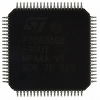
PSD835G2-90UI STMicroelectronics, PSD835G2-90UI Datasheet - Page 37

PSD835G2-90UI
Manufacturer Part Number
PSD835G2-90UI
Description
IC FLASH 4MBIT 90NS 80TQFP
Manufacturer
STMicroelectronics
Datasheet
1.PSD835G2-90U.pdf
(120 pages)
Specifications of PSD835G2-90UI
Format - Memory
FLASH
Memory Type
FLASH
Memory Size
4M (512K x 8)
Speed
90ns
Interface
Parallel
Voltage - Supply
4.5 V ~ 5.5 V
Operating Temperature
-40°C ~ 85°C
Package / Case
80-TQFP, 80-VQFP
Lead Free Status / RoHS Status
Lead free / RoHS Compliant
Other names
497-2016
Available stocks
Company
Part Number
Manufacturer
Quantity
Price
Company:
Part Number:
PSD835G2-90UI
Manufacturer:
ST
Quantity:
201
Company:
Part Number:
PSD835G2-90UI
Manufacturer:
STMicroelectronics
Quantity:
10 000
PSD835G2
7
7.1
7.2
Instructions
An instruction consists of a sequence of specific operations. Each received byte is
sequentially decoded by the PSD and not executed as a standard WRITE operation. The
instruction is executed when the correct number of bytes is properly received and the time
between two consecutive bytes is shorter than the time-out period. Some instructions are
structured to include READ operations after the initial WRITE operations.
The instruction must be followed exactly. Any invalid combination of instruction bytes or
time-out between two consecutive bytes while addressing Flash memory resets the device
logic into READ mode (Flash memory is read like a ROM device).
The PSD supports the instructions summarized in
●
●
●
●
●
●
●
These instructions are detailed in
two bytes of an instruction are the coded cycles and are followed by an instruction byte or a
confirmation byte. The coded cycles consist in writing the data AAh to address X555h
during the first cycle and data 55h to address XAAAh during the second cycle unless the
Bypass Instruction feature is used). Address signals A15-A12 are Don’t Care during the
instruction WRITE cycles. However, the appropriate Sector Select (FS0-FS7 or CSBOOT0-
CSBOOT3) must be selected.
The primary and secondary Flash memories have the same instruction set (except for Read
Primary Flash Identifier). The Sector Select signals determine which Flash memory is to
receive and execute the instruction. The primary Flash memory is selected if any one of
Sector Select (FS0-FS7) is high, and the secondary Flash memory is selected if any one of
Sector Select (CSBOOT0-CSBOOT3) is high.
Power-up mode
The PSD internal logic is reset upon Power-up to the READ mode. Sector Select (FS0-FS7
and CSBOOT0-CSBOOT3) must be held low, and Write Strobe (WR, CNTL0) high, during
Power-up for maximum security of the data contents and to remove the possibility of a byte
being written on the first edge of Write Strobe (WR, CNTL0). Any WRITE cycle initiation is
locked when V
READ
Under typical conditions, the MCU may read the primary Flash memory or the secondary
Flash memory using READ operations just as it would a ROM or RAM device. Alternately,
the MCU may use READ operations to obtain status information about a Program or Erase
Erase memory by chip or sector
Suspend or resume sector erase
Program a byte
Reset to READ mode
Read primary Flash Identifier value
Read Sector Protection Status
Bypass
CC
is below V
LKO
.
Table
7. For efficient decoding of the instructions, the first
Table
7:
Instructions
37/120


