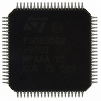
PSD835G2-90UI STMicroelectronics, PSD835G2-90UI Datasheet - Page 16

PSD835G2-90UI
Manufacturer Part Number
PSD835G2-90UI
Description
IC FLASH 4MBIT 90NS 80TQFP
Manufacturer
STMicroelectronics
Datasheet
1.PSD835G2-90U.pdf
(120 pages)
Specifications of PSD835G2-90UI
Format - Memory
FLASH
Memory Type
FLASH
Memory Size
4M (512K x 8)
Speed
90ns
Interface
Parallel
Voltage - Supply
4.5 V ~ 5.5 V
Operating Temperature
-40°C ~ 85°C
Package / Case
80-TQFP, 80-VQFP
Lead Free Status / RoHS Status
Lead free / RoHS Compliant
Other names
497-2016
Available stocks
Company
Part Number
Manufacturer
Quantity
Price
Company:
Part Number:
PSD835G2-90UI
Manufacturer:
ST
Quantity:
201
Company:
Part Number:
PSD835G2-90UI
Manufacturer:
STMicroelectronics
Quantity:
10 000
Description
Table 1.
16/120
PF0-PF7
name
PD3
PE0
PE1
PE2
PE3
PE4
PE5
PE6
PE7
Pin
31-38
Pin
Pin description (continued)
71
72
73
74
75
76
77
78
2
I/O CMOS
I/O CMOS
I/O CMOS
I/O CMOS
I/O CMOS
I/O CMOS
I/O CMOS
I/O CMOS
I/O CMOS
I/O CMOS
or Open
or Open
or Open
or Open
or Open
or Open
or Open
or Open
or Open
or Open
Drain
Drain
Drain
Drain
Drain
Drain
Drain
Drain
Drain
Drain
Type
PD3 pin of port D. This port pin can be configured to have the following functions:
MCU I/O – write to or read from a standard output or input port.
Input to the PLDs.
PE0 pin of port E. This port pin can be configured to have the following functions:
MCU I/O – write to or read from a standard output or input port.
Latched address output.
TMS input for JTAG/ISP interface.
PE1 pin of port E. This port pin can be configured to have the following functions:
MCU I/O – write to or read from a standard output or input port.
Latched address output.
TCK input for JTAG/ISP interface (Schmidt Trigger).
PE2 pin of port E. This port pin can be configured to have the following functions:
MCU I/O – write to or read from a standard output or input port.
Latched address output.
TDI input for JTAG/ISP interface.
PE3 pin of port E. This port pin can be configured to have the following functions:
MCU I/O – write to or read from a standard output or input port.
Latched address output.
TDO input for JTAG/ISP interface.
PE4 pin of port E. This port pin can be configured to have the following functions:
MCU I/O – write to or read from a standard output or input port.
Latched address output.
TSTAT input for the ISP interface.
Ready/Busy for in-circuit Parallel Programming.
PE5 pin of port E. This port pin can be configured to have the following functions:
MCU I/O – write to or read from a standard output or input port.
Latched address output.
TERR active low input for ISP interface.
PE6 pin of port E. This port pin can be configured to have the following functions:
MCU I/O – write to or read from a standard output or input port.
Latched address output.
PE7 pin of port E. This port pin can be configured to have the following functions:
MCU I/O – write to or read from a standard output or input port.
Latched address output.
PF0 through PF7 pins of port F. This port pins can be configured to have the
following functions:
MCU I/O – write to or read from a standard output or input port.
Input to the PLDs.
Latched address outputs.
As address A0-A3 inputs in 80C51XA mode.
As data bus port (D07) in non-multiplexed bus configuration.
Description
PSD835G2


