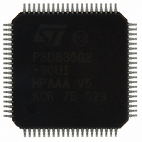
PSD835G2-90UI STMicroelectronics, PSD835G2-90UI Datasheet - Page 83

PSD835G2-90UI
Manufacturer Part Number
PSD835G2-90UI
Description
IC FLASH 4MBIT 90NS 80TQFP
Manufacturer
STMicroelectronics
Datasheet
1.PSD835G2-90U.pdf
(120 pages)
Specifications of PSD835G2-90UI
Format - Memory
FLASH
Memory Type
FLASH
Memory Size
4M (512K x 8)
Speed
90ns
Interface
Parallel
Voltage - Supply
4.5 V ~ 5.5 V
Operating Temperature
-40°C ~ 85°C
Package / Case
80-TQFP, 80-VQFP
Lead Free Status / RoHS Status
Lead free / RoHS Compliant
Other names
497-2016
Available stocks
Company
Part Number
Manufacturer
Quantity
Price
Company:
Part Number:
PSD835G2-90UI
Manufacturer:
ST
Quantity:
201
Company:
Part Number:
PSD835G2-90UI
Manufacturer:
STMicroelectronics
Quantity:
10 000
PSD835G2
17.17
17.18
17.19
17.20
17.21
Output macrocells (OMC)
The CPLD output macrocells (OMC) occupy a location in the MCU’s address space. The
MCU can read the output of the output macrocells (OMC). If the OMC Mask register bits are
not set, writing to the macrocell loads data to the macrocell flip-flops (see
PLDs).
OMC Mask register
Each OMC Mask register bit corresponds to an Output macrocell (OMC) flip-flop. When the
OMC Mask register bit is set to a '1,' loading data into the Output macrocell (OMC) flip-flop
is blocked. The default value is 0 or unblocked.
Table 22.
Input macrocells (IMC)
The input macrocells (IMC) can be used to latch or store external inputs. The outputs of the
input macrocells (IMC) are routed to the PLD input bus, and can be read by the MCU (see
Section 15:
Enable Out
The Enable Out register can be read by the MCU. It contains the output enable values for a
given port. A ‘1’ indicates the driver is in output mode. A ‘0’ indicates the driver is in tri-state
and the pin is in input mode.
Ports A,B and C – functionality and structure
Ports A and B have similar functionality and structure, as shown in
Data In
Data Out
Output macrocell
Mask macrocell
Input macrocell
Enable Out
Register name
PLDs).
Port Data registers
A, B, C, D, E, F,
G
A, B, C, D, E, F,
G
A, B
A, B
A, B, C
A, B, C, F
Port
READ – input on pin
WRITE/READ
READ – outputs of macrocells
WRITE – loading macrocell flip-flops
WRITE/READ – prevents loading into a given
macrocell
READ – outputs of the input macrocells
READ – the output enable control of the port driver
MCU access
Figure
Section 15:
27.
I/O ports
83/120


