MPC8313E-RDB Freescale Semiconductor, MPC8313E-RDB Datasheet - Page 44
MPC8313E-RDB
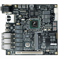
Manufacturer Part Number
MPC8313E-RDB
Description
BOARD PROCESSOR
Manufacturer
Freescale Semiconductor
Series
PowerQUICC II™ PROr
Type
MCUr
Datasheets
1.MPC8313CZQAFFB.pdf
(100 pages)
2.MPC8313E-RDBB.pdf
(52 pages)
3.MPC8313E-RDBB.pdf
(2 pages)
Specifications of MPC8313E-RDB
Contents
Reference Design Board, Software and Documentation
Termination Type
SMD
Supply Voltage Max
1.05V
Tool / Board Applications
Wired Connectivity-LIN, CAN, Ethernet, USB
Mcu Supported Families
POWERQUICC II PRO
Rohs Compliant
Yes
Filter Terminals
SMD
Silicon Manufacturer
Freescale
Silicon Core Number
MPC83xx
Kit Application Type
Communication & Networking
Application Sub Type
Ethernet
Core Architecture
Power Architecture
Silicon Family Name
PowerQUICC II PRO
For Use With/related Products
MPC8313E
Lead Free Status / RoHS Status
Lead free / RoHS Compliant


High-Speed Serial Interfaces (HSSI)
The other detailed AC requirements of the SerDes reference clocks is defined by each interface protocol
based on application usage. Refer to the following section for detailed information:
9.2.4.1
SD_REF_CLK/SD_REF_CLK are not intended to be used with, and should not be clocked by, a spread
spectrum clock source.
44
At recommended operating conditions with XV
Rising edge rate (SDn_REF_CLK) to falling edge rate
(SDn_REF_CLK) matching
Notes:
1. Measurement taken from single-ended waveform.
2. Measurement taken from differential waveform.
3. Measured from –200 to +200 mV on the differential waveform (derived from SD n _REF_CLK minus SD n _REF_CLK). The
4. Matching applies to rising edge rate for SD n _REF_CLK and falling edge rate for SD n _REF_CLK. It is measured using a
signal must be monotonic through the measurement region for rise and fall time. The 400 mV measurement window is
centered on the differential zero crossing. See
200 mV window centered on the median cross point, where SD n _REF_CLK rising meets SD n _REF_CLK falling. The median
cross point is used to calculate the voltage thresholds the oscilloscope is to use for the edge rate calculations. The rise edge
rate of SD n _REF_CLK should be compared to the fall edge rate of SD n _REF_CLK, the maximum allowed difference should
not exceed 20% of the slowest edge rate. See
•
SD n _REF_CLK
SD n _REF_CLK
V
V
IH
IL
SD n _REF_CLK
SD n _REF_CLK
SD n _REF_CLK
V
Section 8.3.2, “AC Requirements for SGMII SD_REF_CLK and SD_REF_CLK”
= +200 mV
= –200 mV
CROSS MEDIAN
Minus
0.0 V
Spread Spectrum Clock
Figure 32. Single-Ended Measurement Points for Rise and Fall Time Matching
Table 40. SerDes Reference Clock Common AC Parameters (continued)
MPC8313E PowerQUICC
Figure 31. Differential Measurement Points for Rise and Fall Time
Parameter
Rise Edge Rage
DD_SRDS1
™
Figure
Figure
or XV
II Pro Processor Hardware Specifications, Rev. 3
DD_SRDS2
31.
32.
V
V
CROSS MEDIAN
CROSS MEDIAN
= 1.0 V ± 5%.
matching
Symbol
Rise-fall
SD n _REF_CLK
SD n _REF_CLK
V
CROSS MEDIAN
+ 100 mV
– 100 mV
Min
—
Fall Edge Rate
T
FALL
Max
20
Freescale Semiconductor
T
RISE
Unit
%
Notes
1, 4
Related parts for MPC8313E-RDB
Image
Part Number
Description
Manufacturer
Datasheet
Request
R

Part Number:
Description:
Mpc8313e Powerquicc Ii Pro Processor
Manufacturer:
Freescale Semiconductor, Inc
Datasheet:

Part Number:
Description:
BOARD CPU 8313E VER 2.1
Manufacturer:
Freescale Semiconductor
Datasheet:

Part Number:
Description:
BOARD CPU 8313E VER 2.2
Manufacturer:
Freescale Semiconductor
Datasheet:
Part Number:
Description:
Microprocessors - MPU 8313 REV2.2 PB ENC EXT
Manufacturer:
Freescale Semiconductor
Datasheet:
Part Number:
Description:
Microprocessors - MPU 8313 REV2.2 PB W/ENC
Manufacturer:
Freescale Semiconductor
Datasheet:
Part Number:
Description:
Microprocessors - MPU 8313 REV2.2 PB NO EN EXT
Manufacturer:
Freescale Semiconductor
Datasheet:
Part Number:
Description:
Microprocessors - MPU 8313 REV2.2 PB NO ENC
Manufacturer:
Freescale Semiconductor
Datasheet:
Part Number:
Description:
Manufacturer:
Freescale Semiconductor, Inc
Datasheet:
Part Number:
Description:
Manufacturer:
Freescale Semiconductor, Inc
Datasheet:
Part Number:
Description:
Manufacturer:
Freescale Semiconductor, Inc
Datasheet:
Part Number:
Description:
Manufacturer:
Freescale Semiconductor, Inc
Datasheet:
Part Number:
Description:
Manufacturer:
Freescale Semiconductor, Inc
Datasheet:
Part Number:
Description:
Manufacturer:
Freescale Semiconductor, Inc
Datasheet:
Part Number:
Description:
Manufacturer:
Freescale Semiconductor, Inc
Datasheet:
Part Number:
Description:
Manufacturer:
Freescale Semiconductor, Inc
Datasheet: