MPC8313E-RDB Freescale Semiconductor, MPC8313E-RDB Datasheet - Page 63
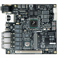
MPC8313E-RDB
Manufacturer Part Number
MPC8313E-RDB
Description
BOARD PROCESSOR
Manufacturer
Freescale Semiconductor
Series
PowerQUICC II™ PROr
Type
MCUr
Datasheets
1.MPC8313CZQAFFB.pdf
(100 pages)
2.MPC8313E-RDBB.pdf
(52 pages)
3.MPC8313E-RDBB.pdf
(2 pages)
Specifications of MPC8313E-RDB
Contents
Reference Design Board, Software and Documentation
Termination Type
SMD
Supply Voltage Max
1.05V
Tool / Board Applications
Wired Connectivity-LIN, CAN, Ethernet, USB
Mcu Supported Families
POWERQUICC II PRO
Rohs Compliant
Yes
Filter Terminals
SMD
Silicon Manufacturer
Freescale
Silicon Core Number
MPC83xx
Kit Application Type
Communication & Networking
Application Sub Type
Ethernet
Core Architecture
Power Architecture
Silicon Family Name
PowerQUICC II PRO
For Use With/related Products
MPC8313E
Lead Free Status / RoHS Status
Lead free / RoHS Compliant


Figure 55
19 Package and Pin Listings
This section details package parameters, pin assignments, and dimensions. The MPC8313E is available in
a thermally enhanced plastic ball grid array (TEPBGAII), see
MPC8313E TEPBGAII,”
information on the TEPBGAII.
19.1
The package parameters are as provided in the following list. The package type is 27 mm × 27 mm,
516 TEPBGAII.
Freescale Semiconductor
Package outline
Interconnects
Pitch
Module height (typical)
Solder Balls
Ball diameter (typical)
SPICLK (Output)
Package Parameters for the MPC8313E TEPBGAII
shows the SPI timing in master mode (internal clock).
Output Signals:
Note: The clock edge is selectable on SPI.
Input Signals:
(See Note)
(See Note)
SPIMISO
SPIMOSI
MPC8313E PowerQUICC
Figure 55. SPI AC Timing in Master Mode (Internal Clock) Diagram
and
Section 19.2, “Mechanical Dimensions of the MPC8313E TEPBGAII,”
t
NIIVKH
™
II Pro Processor Hardware Specifications, Rev. 3
t
NIKHOV
t
NIIXKH
27 mm × 27 mm
516
1.00 mm
2.25 mm
95.5 Sn/0.5 Cu/4 Ag (VR package),
62 Sn/36 Pb/2 Ag (ZQ package)
0.6 mm
Section 19.1, “Package Parameters for the
Package and Pin Listings
for
63
Related parts for MPC8313E-RDB
Image
Part Number
Description
Manufacturer
Datasheet
Request
R

Part Number:
Description:
Mpc8313e Powerquicc Ii Pro Processor
Manufacturer:
Freescale Semiconductor, Inc
Datasheet:

Part Number:
Description:
BOARD CPU 8313E VER 2.1
Manufacturer:
Freescale Semiconductor
Datasheet:

Part Number:
Description:
BOARD CPU 8313E VER 2.2
Manufacturer:
Freescale Semiconductor
Datasheet:
Part Number:
Description:
Microprocessors - MPU 8313 REV2.2 PB ENC EXT
Manufacturer:
Freescale Semiconductor
Datasheet:
Part Number:
Description:
Microprocessors - MPU 8313 REV2.2 PB W/ENC
Manufacturer:
Freescale Semiconductor
Datasheet:
Part Number:
Description:
Microprocessors - MPU 8313 REV2.2 PB NO EN EXT
Manufacturer:
Freescale Semiconductor
Datasheet:
Part Number:
Description:
Microprocessors - MPU 8313 REV2.2 PB NO ENC
Manufacturer:
Freescale Semiconductor
Datasheet:
Part Number:
Description:
Manufacturer:
Freescale Semiconductor, Inc
Datasheet:
Part Number:
Description:
Manufacturer:
Freescale Semiconductor, Inc
Datasheet:
Part Number:
Description:
Manufacturer:
Freescale Semiconductor, Inc
Datasheet:
Part Number:
Description:
Manufacturer:
Freescale Semiconductor, Inc
Datasheet:
Part Number:
Description:
Manufacturer:
Freescale Semiconductor, Inc
Datasheet:
Part Number:
Description:
Manufacturer:
Freescale Semiconductor, Inc
Datasheet:
Part Number:
Description:
Manufacturer:
Freescale Semiconductor, Inc
Datasheet:
Part Number:
Description:
Manufacturer:
Freescale Semiconductor, Inc
Datasheet: