MPC8313E-RDB Freescale Semiconductor, MPC8313E-RDB Datasheet - Page 91
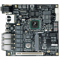
MPC8313E-RDB
Manufacturer Part Number
MPC8313E-RDB
Description
BOARD PROCESSOR
Manufacturer
Freescale Semiconductor
Series
PowerQUICC II™ PROr
Type
MCUr
Datasheets
1.MPC8313CZQAFFB.pdf
(100 pages)
2.MPC8313E-RDBB.pdf
(52 pages)
3.MPC8313E-RDBB.pdf
(2 pages)
Specifications of MPC8313E-RDB
Contents
Reference Design Board, Software and Documentation
Termination Type
SMD
Supply Voltage Max
1.05V
Tool / Board Applications
Wired Connectivity-LIN, CAN, Ethernet, USB
Mcu Supported Families
POWERQUICC II PRO
Rohs Compliant
Yes
Filter Terminals
SMD
Silicon Manufacturer
Freescale
Silicon Core Number
MPC83xx
Kit Application Type
Communication & Networking
Application Sub Type
Ethernet
Core Architecture
Power Architecture
Silicon Family Name
PowerQUICC II PRO
For Use With/related Products
MPC8313E
Lead Free Status / RoHS Status
Lead free / RoHS Compliant


The value of this resistance and the strength of the driver’s current source can be found by making two
measurements. First, the output voltage is measured while driving logic 1 without an external differential
termination resistor. The measured voltage is V
while driving logic 1 with an external precision differential termination resistor of value R
measured voltage is V
R
Table 72
nominal NV
22.7
The MPC8313E provides the user with power-on configuration options which can be set through the use
of external pull-up or pull-down resistors of 4.7 kΩ on certain output pins (see customer visible
configuration pins). These pins are generally used as output only pins in normal operation.
While HRESET is asserted however, these pins are treated as inputs. The value presented on these pins
while HRESET is asserted, is latched when PORESET deasserts, at which time the input receiver is
disabled and the I/O circuit takes on its normal function. Careful board layout with stubless connections
to these pull-up/pull-down resistors coupled with the large value of the pull-up/pull-down resistor should
minimize the disruption of signal quality or speed for output pins thus configured.
Freescale Semiconductor
Note: Nominal supply voltages. See
term
Impedance
Differential
R
R
× (V
N
P
summarizes the signal impedance targets. The driver impedance are targeted at minimum V
Configuration Pin Muxing
1
/V
DD
2
, 105°C.
– 1). The drive current is then I
Configuration, Power
Local Bus, Ethernet,
DUART, Control,
MPC8313E PowerQUICC
Management
42 Target
42 Target
2
= (1/(1/R
NA
Table
Figure 60. Driver Impedance Measurement
1
Data
+ 1/R
Table 72. Impedance Characteristics
1, T
(Not Including PCI
J
Output Clocks)
2
= 105°C.
™
)) × I
PCI Signals
II Pro Processor Hardware Specifications, Rev. 3
25 Target
25 Target
NA
1
source
source
= R
source
. Solving for the output impedance gives R
= V
1
× I
PCI Output Clocks
/R
PCI_SYNC_OUT)
Pad
source
R
source
R
NV
(Including
N
P
42 Target
42 Target
V
SS
DD
NA
. Second, the output voltage is measured
.
SW2
SW1
DDR DRAM
20 Target
20 Target
NA
System Design Information
Symbol
Z
term
DIFF
Z
Z
0
0
. The
source
Unit
=
Ω
Ω
Ω
DD
91
,
Related parts for MPC8313E-RDB
Image
Part Number
Description
Manufacturer
Datasheet
Request
R

Part Number:
Description:
Mpc8313e Powerquicc Ii Pro Processor
Manufacturer:
Freescale Semiconductor, Inc
Datasheet:

Part Number:
Description:
BOARD CPU 8313E VER 2.1
Manufacturer:
Freescale Semiconductor
Datasheet:

Part Number:
Description:
BOARD CPU 8313E VER 2.2
Manufacturer:
Freescale Semiconductor
Datasheet:
Part Number:
Description:
Microprocessors - MPU 8313 REV2.2 PB ENC EXT
Manufacturer:
Freescale Semiconductor
Datasheet:
Part Number:
Description:
Microprocessors - MPU 8313 REV2.2 PB W/ENC
Manufacturer:
Freescale Semiconductor
Datasheet:
Part Number:
Description:
Microprocessors - MPU 8313 REV2.2 PB NO EN EXT
Manufacturer:
Freescale Semiconductor
Datasheet:
Part Number:
Description:
Microprocessors - MPU 8313 REV2.2 PB NO ENC
Manufacturer:
Freescale Semiconductor
Datasheet:
Part Number:
Description:
Manufacturer:
Freescale Semiconductor, Inc
Datasheet:
Part Number:
Description:
Manufacturer:
Freescale Semiconductor, Inc
Datasheet:
Part Number:
Description:
Manufacturer:
Freescale Semiconductor, Inc
Datasheet:
Part Number:
Description:
Manufacturer:
Freescale Semiconductor, Inc
Datasheet:
Part Number:
Description:
Manufacturer:
Freescale Semiconductor, Inc
Datasheet:
Part Number:
Description:
Manufacturer:
Freescale Semiconductor, Inc
Datasheet:
Part Number:
Description:
Manufacturer:
Freescale Semiconductor, Inc
Datasheet:
Part Number:
Description:
Manufacturer:
Freescale Semiconductor, Inc
Datasheet: