MPC8313E-RDB Freescale Semiconductor, MPC8313E-RDB Datasheet - Page 51
MPC8313E-RDB
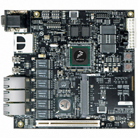
Manufacturer Part Number
MPC8313E-RDB
Description
BOARD PROCESSOR
Manufacturer
Freescale Semiconductor
Series
PowerQUICC II™ PROr
Type
MCUr
Datasheets
1.MPC8313CZQAFFB.pdf
(100 pages)
2.MPC8313E-RDBB.pdf
(52 pages)
3.MPC8313E-RDBB.pdf
(2 pages)
Specifications of MPC8313E-RDB
Contents
Reference Design Board, Software and Documentation
Termination Type
SMD
Supply Voltage Max
1.05V
Tool / Board Applications
Wired Connectivity-LIN, CAN, Ethernet, USB
Mcu Supported Families
POWERQUICC II PRO
Rohs Compliant
Yes
Filter Terminals
SMD
Silicon Manufacturer
Freescale
Silicon Core Number
MPC83xx
Kit Application Type
Communication & Networking
Application Sub Type
Ethernet
Core Architecture
Power Architecture
Silicon Family Name
PowerQUICC II PRO
For Use With/related Products
MPC8313E
Lead Free Status / RoHS Status
Lead free / RoHS Compliant


12 JTAG
This section describes the DC and AC electrical specifications for the IEEE Std 1149.1™ (JTAG)
interface.
12.1
Table 47
12.2
This section describes the AC electrical specifications for the IEEE Std 1149.1 (JTAG) interface.
Table 48
Freescale Semiconductor
At recommended operating conditions (see
Input high voltage
Input low voltage
Input current
Output high voltage
Output low voltage
Output low voltage
JTAG external clock frequency of operation
JTAG external clock cycle time
JTAG external clock pulse width measured at 1.4 V
JTAG external clock rise and fall times
TRST assert time
Input setup times:
Input hold times:
Valid times:
provides the DC electrical characteristics for the IEEE Std 1149.1 (JTAG) interface.
provides the JTAG AC timing specifications as defined in
JTAG DC Electrical Characteristics
JTAG AC Timing Specifications
Characteristic
Table 48. JTAG AC Timing Specifications (Independent of SYS_CLK_IN)
MPC8313E PowerQUICC
Parameter
Table 47. JTAG Interface DC Electrical Characteristics
Boundary-scan data
Boundary-scan data
Boundary-scan data
Table
2).
™
TMS, TDI
TMS, TDI
II Pro Processor Hardware Specifications, Rev. 3
Symbol
V
V
V
TDO
V
V
I
IN
OH
OL
OL
IH
IL
t
JTGR
Symbol
t
t
t
t
t
t
t
JTDVKH
JTDXKH
JTKHKL
JTKLDV
JTKLOV
t
JTIVKH
JTIXKH
t
TRST
f
I
JTG
OH
I
JTG
I
& t
OL
OL
Condition
JTGF
= –8.0 mA
= 3.2 mA
= 8.0 mA
2
—
—
—
Min
Figure 41
30
15
25
10
10
0
0
4
4
2
2
–0.3
Min
2.1
2.4
—
—
—
through
Max
33.3
11
11
—
—
—
—
—
—
—
2
NV
Figure
DD
1
Max
0.8
0.5
0.4
±5
—
MHz
+ 0.3
Unit
ns
ns
ns
ns
ns
ns
ns
45.
Notes
Unit
μA
V
V
V
V
V
4
4
5
3
JTAG
51
Related parts for MPC8313E-RDB
Image
Part Number
Description
Manufacturer
Datasheet
Request
R

Part Number:
Description:
Mpc8313e Powerquicc Ii Pro Processor
Manufacturer:
Freescale Semiconductor, Inc
Datasheet:

Part Number:
Description:
BOARD CPU 8313E VER 2.1
Manufacturer:
Freescale Semiconductor
Datasheet:

Part Number:
Description:
BOARD CPU 8313E VER 2.2
Manufacturer:
Freescale Semiconductor
Datasheet:
Part Number:
Description:
Microprocessors - MPU 8313 REV2.2 PB ENC EXT
Manufacturer:
Freescale Semiconductor
Datasheet:
Part Number:
Description:
Microprocessors - MPU 8313 REV2.2 PB W/ENC
Manufacturer:
Freescale Semiconductor
Datasheet:
Part Number:
Description:
Microprocessors - MPU 8313 REV2.2 PB NO EN EXT
Manufacturer:
Freescale Semiconductor
Datasheet:
Part Number:
Description:
Microprocessors - MPU 8313 REV2.2 PB NO ENC
Manufacturer:
Freescale Semiconductor
Datasheet:
Part Number:
Description:
Manufacturer:
Freescale Semiconductor, Inc
Datasheet:
Part Number:
Description:
Manufacturer:
Freescale Semiconductor, Inc
Datasheet:
Part Number:
Description:
Manufacturer:
Freescale Semiconductor, Inc
Datasheet:
Part Number:
Description:
Manufacturer:
Freescale Semiconductor, Inc
Datasheet:
Part Number:
Description:
Manufacturer:
Freescale Semiconductor, Inc
Datasheet:
Part Number:
Description:
Manufacturer:
Freescale Semiconductor, Inc
Datasheet:
Part Number:
Description:
Manufacturer:
Freescale Semiconductor, Inc
Datasheet:
Part Number:
Description:
Manufacturer:
Freescale Semiconductor, Inc
Datasheet: