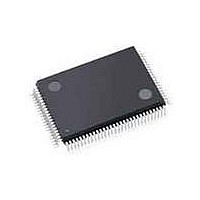
C8051F060-TB Silicon Laboratories Inc, C8051F060-TB Datasheet - Page 320

C8051F060-TB
Manufacturer Part Number
C8051F060-TB
Description
BOARD PROTOTYPING W/C8051F060
Manufacturer
Silicon Laboratories Inc
Type
MCUr
Specifications of C8051F060-TB
Contents
Board
Processor To Be Evaluated
C8051F06x
Interface Type
USB
Lead Free Status / RoHS Status
Contains lead / RoHS non-compliant
For Use With/related Products
C8051F060
Lead Free Status / Rohs Status
Lead free / RoHS Compliant
- Current page: 320 of 328
- Download datasheet (2Mb)
C8051F060/1/2/3/4/5/6/7
320
EXTEST provides access to both capture and update actions, while Sample only performs a capture.
24, 26, 28, 30, 32,
25, 27, 29, 31, 33,
40, 42, 44, 46, 48,
41, 43, 45, 47, 49,
56, 58, 60, 62, 64,
57, 59, 61, 63, 65,
74, 76, 78, 80, 82,
75, 77, 79, 81, 83,
86, 88, 90, 92, 94,
8, 10, 12, 14, 16,
9, 11, 13, 15, 17,
96, 98, 100
50, 52, 54
51, 53, 55
66, 68, 70
67, 69, 71
18, 20, 22
19, 21, 23
34, 36, 38
35, 37, 39
Bit
72
73
84
85
0
1
2
3
4
5
6
7
Table 26.2. Boundary Data Register Bit Definitions (C8051F061/3/5/7)
Action
Capture Not used
Update
Capture Not used
Update
Capture CAN RX Output Enable to pin
Update
Capture CAN RX Input from pin
Update
Capture CAN TX Output Enable to pin
Update
Capture CAN TX Input from pin
Update
Capture External Clock from XTAL1 pin
Update
Capture Weak Pullup Enable from MCU
Update
Capture P0.n output enable from MCU (e.g. Bit 8 = P0.0, Bit 10 = P0.1, etc.)
Update
Capture P0.n input from pin (e.g. Bit 9 = P0.0, Bit 11 = P0.1, etc.)
Update
Capture P1.n output enable from MCU (follows P0.n numbering scheme)
Update
Capture P1.n input from pin (follows P0.n numbering scheme)
Update
Capture P2.n output enable from MCU (follows P0.n numbering scheme)
Update
Capture P2.n input from pin (follows P0.n numbering scheme)
Update
Capture P3.n output enable from MCU (follows P0.n numbering scheme)
Update
Capture P3.n input from pin (follows P0.n numbering scheme)
Update
Capture Reset Enable from MCU
Update
Capture Reset Input from /RST pin
Update
Capture P5.0, P5.1, P5.2, P5.3, P5.5, P5.7 (respectively) output enable from
Update
Capture P5.0, P5.1, P5.2, P5.3, P5.5, P5.7 (respectively) input from pin†
Update
Capture P6.n output enable from MCU (follows P0.n numbering scheme)†
Update
Target
Not used
Not used
CAN RX Output Enable to pin
CAN RX Output to pin
CAN TX Output Enable to pin
CAN TX Output to pin
Not used
Weak Pullup Enable to Port Pins
P0.n output enable to pin (e.g. Bit 8 = P0.0oe, Bit 10 = P0.1oe, etc.)
P0.n output to pin (e.g. Bit 9 = P0.0, Bit 11 = P0.1, etc.)
P1.n output enable to pin (follows P0.n numbering scheme)
P1.n output to pin (follows P0.n numbering scheme)
P2.n output enable to pin (follows P0.n numbering scheme)
P2.n output to pin (follows P0.n numbering scheme)
P3.n output enable to pin (follows P0.n numbering scheme)
P3.n output to pin (follows P0.n numbering scheme)
Reset Enable to /RST pin
Not used
MCU†
P5.0, P5.1, P5.2, P5.3, P5.5, P5.7 (respectively) output enable to pin†
P5.0, P5.1, P5.2, P5.3, P5.5, P5.7 (respectively) output to pin†
P6.n output enable to pin (follows P0.n numbering scheme)†
Rev. 1.2
Related parts for C8051F060-TB
Image
Part Number
Description
Manufacturer
Datasheet
Request
R
Part Number:
Description:
SMD/C°/SINGLE-ENDED OUTPUT SILICON OSCILLATOR
Manufacturer:
Silicon Laboratories Inc
Part Number:
Description:
Manufacturer:
Silicon Laboratories Inc
Datasheet:
Part Number:
Description:
N/A N/A/SI4010 AES KEYFOB DEMO WITH LCD RX
Manufacturer:
Silicon Laboratories Inc
Datasheet:
Part Number:
Description:
N/A N/A/SI4010 SIMPLIFIED KEY FOB DEMO WITH LED RX
Manufacturer:
Silicon Laboratories Inc
Datasheet:
Part Number:
Description:
N/A/-40 TO 85 OC/EZLINK MODULE; F930/4432 HIGH BAND (REV E/B1)
Manufacturer:
Silicon Laboratories Inc
Part Number:
Description:
EZLink Module; F930/4432 Low Band (rev e/B1)
Manufacturer:
Silicon Laboratories Inc
Part Number:
Description:
I°/4460 10 DBM RADIO TEST CARD 434 MHZ
Manufacturer:
Silicon Laboratories Inc
Part Number:
Description:
I°/4461 14 DBM RADIO TEST CARD 868 MHZ
Manufacturer:
Silicon Laboratories Inc
Part Number:
Description:
I°/4463 20 DBM RFSWITCH RADIO TEST CARD 460 MHZ
Manufacturer:
Silicon Laboratories Inc
Part Number:
Description:
I°/4463 20 DBM RADIO TEST CARD 868 MHZ
Manufacturer:
Silicon Laboratories Inc
Part Number:
Description:
I°/4463 27 DBM RADIO TEST CARD 868 MHZ
Manufacturer:
Silicon Laboratories Inc
Part Number:
Description:
I°/4463 SKYWORKS 30 DBM RADIO TEST CARD 915 MHZ
Manufacturer:
Silicon Laboratories Inc
Part Number:
Description:
N/A N/A/-40 TO 85 OC/4463 RFMD 30 DBM RADIO TEST CARD 915 MHZ
Manufacturer:
Silicon Laboratories Inc
Part Number:
Description:
I°/4463 20 DBM RADIO TEST CARD 169 MHZ
Manufacturer:
Silicon Laboratories Inc


