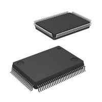
R5F363AENFA#U0 Renesas Electronics America, R5F363AENFA#U0 Datasheet - Page 525

R5F363AENFA#U0
Manufacturer Part Number
R5F363AENFA#U0
Description
MCU 4KB FLASH 256/16K 100-QFP
Manufacturer
Renesas Electronics America
Series
M16C/60/63r
Specifications of R5F363AENFA#U0
Core Processor
M16C/60
Core Size
16/32-Bit
Speed
20MHz
Connectivity
EBI/EMI, I²C, SIO, UART/USART
Peripherals
DMA, LVD, POR, PWM, WDT
Number Of I /o
85
Program Memory Size
256KB (256K x 8)
Program Memory Type
FLASH
Ram Size
20K x 8
Voltage - Supply (vcc/vdd)
1.8 V ~ 5.5 V
Data Converters
A/D 26x10b; D/A 2x8b
Oscillator Type
Internal
Operating Temperature
-20°C ~ 85°C
Package / Case
100-QFP
Lead Free Status / RoHS Status
Lead free / RoHS Compliant
Eeprom Size
-
Available stocks
Company
Part Number
Manufacturer
Quantity
Price
- Current page: 525 of 883
- Download datasheet (13Mb)
M16C/63 Group
REJ09B0510-0100 Rev.1.00 Sep 15, 2009
Page 487 of 836
23.3
23.3.1
Table 23.5
Data format
Transmit/receive clock
Transmit/receive control
Transmission start conditions
Reception start conditions
Interrupt request
generation timing
Error detection
Selectable functions
i = 0 to 2, 5 to 7
Notes:
The clock synchronous serial I/O mode uses a transmit/receive clock to transmit/receive data. Table
23.5 lists the Clock Synchronous Serial I/O Mode Specifications.
1.
2.
Operations
When an external clock is selected, either of the following conditions must be met: If the CKPOL bit in the
UiC0 register is 0 (transmit data output at the falling edge and the receive data taken in at the rising edge of
the transmit/receive clock), the external clock is in the high state; if the CKPOL bit in the UiC0 register is 1
(transmit data output at the rising edge and the receive data taken in at the falling edge of the
transmit/receive clock), the external clock is in the low state.
If an overrun error occurs, the receive data of the UiRB register will be undefined. The IR bit in the SiRIC
register remains unchanged.
Clock Synchronous Serial I/O Mode
Item
Clock Synchronous Serial I/O Mode Specifications
Character length: 8 bits
Selectable from CTS function, RTS function, or CTS/RTS function disabled
To start transmission, satisfy the following requirements
To start reception, satisfy the following requirements
Transmit interrupt: One of the following can be selected.
Receive interrupt:
Overrun error
•
•
•
•
•
•
•
•
•
•
•
•
•
•
•
•
•
CKDIR bit in the UiMR register = 0 (internal clock):
fj = f1SIO, f2SIO, f8SIO, f32SIO
CKDIR bit = 1 (external clock): Input from CLKi pin
The TE bit in the UiC1 register = 1 (transmission enabled)
The TI bit in the UiC1 register = 0 (data present in UiTB register)
If CTS function is selected, input on the CTSi pin is low.
The RE bit in the UiC1 register = 1 (reception enabled)
The TE bit in the UiC1 register = 1 (transmission enabled)
The TI bit in the UiC1 register = 0 (data present in the UiTB register)
The UiIRS bit in the UiC1 or UCON register = 0 (transmit buffer empty):
When transferring data from the UiTB register to the UARTi transmit register (at start
of transmission)
The UiIRS bit = 1 (transmission completed):
When the serial interface completes sending data from the UARTi transmit register
When transferring data from the UARTi receive register to the UiRB register (at
completion of reception)
This error occurs if the serial interface starts receiving the next unit of data before
reading the UiRB register and receiving the seventh bit of the next unit of data
CLK polarity selection
Data input/output can be selected to occur synchronously with the rising or falling
edge of the transmit/receive clock
LSB first, MSB first selection
Whether to start sending/receiving data beginning with bit 0 or beginning with bit 7
can be selected
Continuous receive mode selection
Reception is enabled immediately by reading the UiRB register
Switching serial data logic
This function reverses the logic value of the transmit/receive data
Transmit/receive clock output from multiple pins selection (UART1)
The output pin can be selected by a program by setting two UART1 transmit/receive
clock pins.
Separate CTS/RTS pins (UART0)
CTS0 and RTS0 are input/output from separate pins
-------------------- -
2 n
(
fj
+
1
)
(2)
Specification
n = Setting value of UiBRG register
23. Serial Interface UARTi (i = 0 to 2, 5 to 7)
(1)
(1)
00h to FFh
Related parts for R5F363AENFA#U0
Image
Part Number
Description
Manufacturer
Datasheet
Request
R

Part Number:
Description:
KIT STARTER FOR M16C/29
Manufacturer:
Renesas Electronics America
Datasheet:

Part Number:
Description:
KIT STARTER FOR R8C/2D
Manufacturer:
Renesas Electronics America
Datasheet:

Part Number:
Description:
R0K33062P STARTER KIT
Manufacturer:
Renesas Electronics America
Datasheet:

Part Number:
Description:
KIT STARTER FOR R8C/23 E8A
Manufacturer:
Renesas Electronics America
Datasheet:

Part Number:
Description:
KIT STARTER FOR R8C/25
Manufacturer:
Renesas Electronics America
Datasheet:

Part Number:
Description:
KIT STARTER H8S2456 SHARPE DSPLY
Manufacturer:
Renesas Electronics America
Datasheet:

Part Number:
Description:
KIT STARTER FOR R8C38C
Manufacturer:
Renesas Electronics America
Datasheet:

Part Number:
Description:
KIT STARTER FOR R8C35C
Manufacturer:
Renesas Electronics America
Datasheet:

Part Number:
Description:
KIT STARTER FOR R8CL3AC+LCD APPS
Manufacturer:
Renesas Electronics America
Datasheet:

Part Number:
Description:
KIT STARTER FOR RX610
Manufacturer:
Renesas Electronics America
Datasheet:

Part Number:
Description:
KIT STARTER FOR R32C/118
Manufacturer:
Renesas Electronics America
Datasheet:

Part Number:
Description:
KIT DEV RSK-R8C/26-29
Manufacturer:
Renesas Electronics America
Datasheet:

Part Number:
Description:
KIT STARTER FOR SH7124
Manufacturer:
Renesas Electronics America
Datasheet:

Part Number:
Description:
KIT STARTER FOR H8SX/1622
Manufacturer:
Renesas Electronics America
Datasheet:

Part Number:
Description:
KIT DEV FOR SH7203
Manufacturer:
Renesas Electronics America
Datasheet:


