R5F363AENFA#U0 Renesas Electronics America, R5F363AENFA#U0 Datasheet - Page 562
R5F363AENFA#U0
Manufacturer Part Number
R5F363AENFA#U0
Description
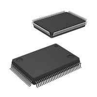
MCU 4KB FLASH 256/16K 100-QFP
Manufacturer
Renesas Electronics America
Series
M16C/60/63r
Specifications of R5F363AENFA#U0
Core Processor
M16C/60
Core Size
16/32-Bit
Speed
20MHz
Connectivity
EBI/EMI, I²C, SIO, UART/USART
Peripherals
DMA, LVD, POR, PWM, WDT
Number Of I /o
85
Program Memory Size
256KB (256K x 8)
Program Memory Type
FLASH
Ram Size
20K x 8
Voltage - Supply (vcc/vdd)
1.8 V ~ 5.5 V
Data Converters
A/D 26x10b; D/A 2x8b
Oscillator Type
Internal
Operating Temperature
-20°C ~ 85°C
Package / Case
100-QFP
Lead Free Status / RoHS Status
Lead free / RoHS Compliant
Eeprom Size
-
Available stocks
Company
Part Number
Manufacturer
Quantity
Price


M16C/63 Group
REJ09B0510-0100 Rev.1.00 Sep 15, 2009
Page 524 of 836
23.3.6
Table 23.26
Data formats
Transmit/receive clock
Transmission start
conditions
Reception start
conditions
Interrupt request
generation timing
Error detection
Notes:
1.
2.
3.
SIM interface devices can communicate in UART mode. Both direct and inverse formats are
available. The TXD2 pin outputs a low-level signal when a parity error is detected.
Table 23.26 lists the SIM Mode Specifications. Table 23.27 lists the Registers Used and Settings in
SIM Mode
When an overrun error occurs, the received data of the U2RB register will be undefined. The IR
bit in the S2RIC register remains unchanged.
After reset, a transmit interrupt request is generated by setting the U2IRS bit to 1 (transmission
completed) and the U2ERE bit to 1 (error signal output) in the U2C1 register. Therefore, when
using SIM mode, set the IR bit to 0 (interrupt not requested) after setting the bits.
The framing error flag and the parity error flag are detected when data is transferred from the
UART2 receive register to the U2RB register.
Item
Special Mode 4 (SIM Mode) (UART2)
SIM Mode Specifications
(1)
(2)
.
To start transmission, satisfy the following requirements.
To start reception, satisfy the following requirements.
•
•
•
•
•
•
•
•
•
•
•
•
•
•
Direct format
Inverse format
The CKDIR bit in the U2MR register = 0 (internal clock): fi/(16(n + 1))
fi = f1SIO, f2SIO, f8SIO, f32SIO
n = Setting value of the U2BRG register 00h to FFh
The CKDIR bit = 1 (external clock): fEXT/(16(n + 1))
fEXT = input from the CLK2 pin
n = Setting value of the U2BRG register 00h to FFh
The TE bit in the U2C1 register
The TI bit in the U2C1 register
The RE bit in the U2C1 register = 1 (reception enabled)
Start bit detection
Transmission
When the serial interface completed sending data from the UART2 transmit
register (the U2IRS bit =1)
Reception
When transferring data from the UART2 receive register to the U2RB register
(at completion of reception)
Overrun error
This error occurs when the serial interface starts receiving the next unit of data
before reading the U2RB register and receives the bit before the last stop bit of
the next unit of data.
Framing error
This error occurs when the number of stop bits set is not detected.
Parity error
During reception, when a parity error is detected, a parity error signal is output
from the TXD2 pin.
During transmission, a parity error is detected by the level of input to the RXD2
pin when a transmission interrupt occurs.
Error sum flag
This flag becomes 1 when an overrun, framing, or parity error occurs.
(3)
(1)
(3)
Specification
= 1 (transmission enabled)
= 0 (data present in the U2TB register)
23. Serial Interface UARTi (i = 0 to 2, 5 to 7)
Related parts for R5F363AENFA#U0
Image
Part Number
Description
Manufacturer
Datasheet
Request
R

Part Number:
Description:
KIT STARTER FOR M16C/29
Manufacturer:
Renesas Electronics America
Datasheet:

Part Number:
Description:
KIT STARTER FOR R8C/2D
Manufacturer:
Renesas Electronics America
Datasheet:

Part Number:
Description:
R0K33062P STARTER KIT
Manufacturer:
Renesas Electronics America
Datasheet:

Part Number:
Description:
KIT STARTER FOR R8C/23 E8A
Manufacturer:
Renesas Electronics America
Datasheet:

Part Number:
Description:
KIT STARTER FOR R8C/25
Manufacturer:
Renesas Electronics America
Datasheet:

Part Number:
Description:
KIT STARTER H8S2456 SHARPE DSPLY
Manufacturer:
Renesas Electronics America
Datasheet:

Part Number:
Description:
KIT STARTER FOR R8C38C
Manufacturer:
Renesas Electronics America
Datasheet:

Part Number:
Description:
KIT STARTER FOR R8C35C
Manufacturer:
Renesas Electronics America
Datasheet:

Part Number:
Description:
KIT STARTER FOR R8CL3AC+LCD APPS
Manufacturer:
Renesas Electronics America
Datasheet:
Part Number:
Description:
KIT STARTER FOR RX610
Manufacturer:
Renesas Electronics America
Datasheet:

Part Number:
Description:
KIT STARTER FOR R32C/118
Manufacturer:
Renesas Electronics America
Datasheet:

Part Number:
Description:
KIT DEV RSK-R8C/26-29
Manufacturer:
Renesas Electronics America
Datasheet:

Part Number:
Description:
KIT STARTER FOR SH7124
Manufacturer:
Renesas Electronics America
Datasheet:

Part Number:
Description:
KIT STARTER FOR H8SX/1622
Manufacturer:
Renesas Electronics America
Datasheet:

Part Number:
Description:
KIT DEV FOR SH7203
Manufacturer:
Renesas Electronics America
Datasheet: