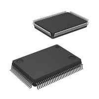
R5F363AENFA#U0 Renesas Electronics America, R5F363AENFA#U0 Datasheet - Page 289

R5F363AENFA#U0
Manufacturer Part Number
R5F363AENFA#U0
Description
MCU 4KB FLASH 256/16K 100-QFP
Manufacturer
Renesas Electronics America
Series
M16C/60/63r
Specifications of R5F363AENFA#U0
Core Processor
M16C/60
Core Size
16/32-Bit
Speed
20MHz
Connectivity
EBI/EMI, I²C, SIO, UART/USART
Peripherals
DMA, LVD, POR, PWM, WDT
Number Of I /o
85
Program Memory Size
256KB (256K x 8)
Program Memory Type
FLASH
Ram Size
20K x 8
Voltage - Supply (vcc/vdd)
1.8 V ~ 5.5 V
Data Converters
A/D 26x10b; D/A 2x8b
Oscillator Type
Internal
Operating Temperature
-20°C ~ 85°C
Package / Case
100-QFP
Lead Free Status / RoHS Status
Lead free / RoHS Compliant
Eeprom Size
-
Available stocks
Company
Part Number
Manufacturer
Quantity
Price
- Current page: 289 of 883
- Download datasheet (13Mb)
M16C/63 Group
REJ09B0510-0100 Rev.1.00 Sep 15, 2009
Page 251 of 836
16.3.3
16.3.3.1
16.3.3.2
16.3.3.3
A transfer cycle is composed of a bus cycle to read data from a source address (source read), and a
bus cycle to write data to a destination address (destination write). The number of read and write bus
cycles depends on the source and destination addresses.
Figure 16.2 shows Transfer Cycles for Source Read Operations. For convenience, the destination write
cycle is shown as one cycle and the source read cycles for the different conditions are shown. In reality,
the destination write cycle is subject to the same conditions as the source read cycle, with the transfer
cycle changing accordingly. When calculating transfer cycles, take into consideration each condition for
the source read and the destination write cycle. For example, when data is transferred in 16-bit units,
and the source address of transfer is an odd address ((2) in Figure 16.2), two source read bus cycles
and two destination write bus cycles are required.
When a 16-bit unit of data is transferred with a 16-bit data bus and the source address starts with an
odd address, the source-read cycle is incremented by one bus cycle, compared to a source address
starting with an even address.
When a 16-bit unit of data is transferred with a 16-bit data bus and the destination address starts with
an odd address, the destination-write cycle is incremented by one bus cycle, compared to a
destination address starting with an even address.
For memory or SFR accesses in which one or more software wait states are inserted, the number of
bus cycles required increases by an amount equal to the number of software wait states.
In memory expansion or microprocessor mode, the transfer cycle is also affected by the BYTE pin
level. Furthermore, the bus cycle itself is extended by a software wait or RDY signal.
If 16 bits of data are transferred on an 8-bit data bus (input to the BYTE pin is high), the operation is
accomplished by transferring 8 bits of data twice. Therefore, this operation requires two bus cycles to
read data and two bus cycles to write data. Furthermore, if the DMAC accesses an internal area
(internal ROM, internal RAM, or SFR), unlike in the case of the CPU, the DMAC uses the data bus
width selected by the BYTE pin.
DMA transfers to and from an external area are affected by the RDY signal. Refer to 11.3.5.6 “ RDY
Signal” for more information.
Transfer Cycles
Effect of Source and Destination Addresses
Effect of Software Wait
Memory Expansion Mode and Microprocessor Mode
16. DMAC
Related parts for R5F363AENFA#U0
Image
Part Number
Description
Manufacturer
Datasheet
Request
R

Part Number:
Description:
KIT STARTER FOR M16C/29
Manufacturer:
Renesas Electronics America
Datasheet:

Part Number:
Description:
KIT STARTER FOR R8C/2D
Manufacturer:
Renesas Electronics America
Datasheet:

Part Number:
Description:
R0K33062P STARTER KIT
Manufacturer:
Renesas Electronics America
Datasheet:

Part Number:
Description:
KIT STARTER FOR R8C/23 E8A
Manufacturer:
Renesas Electronics America
Datasheet:

Part Number:
Description:
KIT STARTER FOR R8C/25
Manufacturer:
Renesas Electronics America
Datasheet:

Part Number:
Description:
KIT STARTER H8S2456 SHARPE DSPLY
Manufacturer:
Renesas Electronics America
Datasheet:

Part Number:
Description:
KIT STARTER FOR R8C38C
Manufacturer:
Renesas Electronics America
Datasheet:

Part Number:
Description:
KIT STARTER FOR R8C35C
Manufacturer:
Renesas Electronics America
Datasheet:

Part Number:
Description:
KIT STARTER FOR R8CL3AC+LCD APPS
Manufacturer:
Renesas Electronics America
Datasheet:

Part Number:
Description:
KIT STARTER FOR RX610
Manufacturer:
Renesas Electronics America
Datasheet:

Part Number:
Description:
KIT STARTER FOR R32C/118
Manufacturer:
Renesas Electronics America
Datasheet:

Part Number:
Description:
KIT DEV RSK-R8C/26-29
Manufacturer:
Renesas Electronics America
Datasheet:

Part Number:
Description:
KIT STARTER FOR SH7124
Manufacturer:
Renesas Electronics America
Datasheet:

Part Number:
Description:
KIT STARTER FOR H8SX/1622
Manufacturer:
Renesas Electronics America
Datasheet:

Part Number:
Description:
KIT DEV FOR SH7203
Manufacturer:
Renesas Electronics America
Datasheet:


