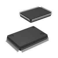
R5F363AENFA#U0 Renesas Electronics America, R5F363AENFA#U0 Datasheet - Page 880

R5F363AENFA#U0
Manufacturer Part Number
R5F363AENFA#U0
Description
MCU 4KB FLASH 256/16K 100-QFP
Manufacturer
Renesas Electronics America
Series
M16C/60/63r
Specifications of R5F363AENFA#U0
Core Processor
M16C/60
Core Size
16/32-Bit
Speed
20MHz
Connectivity
EBI/EMI, I²C, SIO, UART/USART
Peripherals
DMA, LVD, POR, PWM, WDT
Number Of I /o
85
Program Memory Size
256KB (256K x 8)
Program Memory Type
FLASH
Ram Size
20K x 8
Voltage - Supply (vcc/vdd)
1.8 V ~ 5.5 V
Data Converters
A/D 26x10b; D/A 2x8b
Oscillator Type
Internal
Operating Temperature
-20°C ~ 85°C
Package / Case
100-QFP
Lead Free Status / RoHS Status
Lead free / RoHS Compliant
Eeprom Size
-
Available stocks
Company
Part Number
Manufacturer
Quantity
Price
- Current page: 880 of 883
- Download datasheet (13Mb)
Rev.
1.00 Sep 15, 2009
Revision History
Date
282, 286,
290, 295,
327, 329,
202, 202
299, 304
470 to
Page
832
832
833
833
835
836
837
472
123
228
230
230
333
442
518
519
569
12
13
14
91
93
3
6
7
7
7
32.25.2 "φA/D frequency" deleted
32.25.2 “Pin Configuration” partially modified
32.25.10 "Repeat Mode, Repeat Sweep Mode 0, and Repeat Sweep
Mode 1" deleted
32.25.7 “A/D Open-Circuit Detection Assist Function” partially deleted
32.27.3.2 “CPU Rewrite Mode Select” added
32.27.3.10 “Software Command” partially modified
32.27.4.1 “Location of User Boot Mode Program” added
Figure 23.1 to Figure 23.3 “Block Diagram of UART 0 to 2, and UART5 to
UART7” partially modified
Table 1.2 “Specifications for the 100-Pin Package (2/2)” partially modified
Table 1.5 “Product List” partially modified
Figure 1.1 “Part No., with Memory Size and Package” partially modified
Figure 1.2 “Marking Diagram (Top View)” partially modified
Figure 1.3 “Marking Diagram (Top View) (2/2)” added
Figure 1.8 “Pin Assignment for the 100-Pin Package” added
Table 1.6 “Pin Names for the 100-Pin Package (1/2)” partially modified
Table 1.7 “Pin Names for the 100-Pin Package (2/2)” partially modified
8.2.2 “System Clock Control Register 0 (CM0)” partially modified
8.2.3 “System Clock Control Register 1 (CM1)” partially modified
Table 9.8 “Resets and Interrupts to Exit Wait Mode and Conditions for Use”
partially modified
14.2.2 “Interrupt Control Register 1”, 14.2.3 “Interrupt Control Register 2”
partially modified
14.13.3 “NMI Interrupt” partially added
14.13.5 “Rewriting the Interrupt Control Register” partially modified
14.13.6 “Instruction to Rewrite the Interrupt Control Register” added
Table 17.7 “Registers and Their Setting in Timer Mode”
Table 17.9 “Registers and Settings in Event Counter Mode (When Not
Processing Two-Phase Pulse Signal)”
Table 17.11 “Registers and Settings in Event Counter Mode (When
Processing Two-Phase Pulse Signal)”
Table 17.13 “Registers and Settings in One-Shot Timer Mode”
Table 17.15 “Registers and Settings in PWM Mode”
Table 17.17 “Registers and Settings in Programmable Output Mode”
Bit of the TAi1 and TAi modified
Table 18.6 “Registers and Settings in Timer Mode”
Table 18.8 “Registers and Settings in Event Counter Mode”
Table 18.10 “Registers and Settings in Pulse Period/Pulse Width
Measurement Modes”
Bit of the TBi1 and TBi modified
22.3.1.1 “Count Source” partially deleted
Table 23.22 “Special Mode 2 Specifications” partially deleted
Figure 23.22 “Serial Bus Communication Control Example (UART2)”
partially modified
25.2.9 “I2C0 Control Register 2 (S4D0)” MSLAD bit name modified
M16C/63 Group Hardware Manual
C - 6
Description
Summary
Related parts for R5F363AENFA#U0
Image
Part Number
Description
Manufacturer
Datasheet
Request
R

Part Number:
Description:
KIT STARTER FOR M16C/29
Manufacturer:
Renesas Electronics America
Datasheet:

Part Number:
Description:
KIT STARTER FOR R8C/2D
Manufacturer:
Renesas Electronics America
Datasheet:

Part Number:
Description:
R0K33062P STARTER KIT
Manufacturer:
Renesas Electronics America
Datasheet:

Part Number:
Description:
KIT STARTER FOR R8C/23 E8A
Manufacturer:
Renesas Electronics America
Datasheet:

Part Number:
Description:
KIT STARTER FOR R8C/25
Manufacturer:
Renesas Electronics America
Datasheet:

Part Number:
Description:
KIT STARTER H8S2456 SHARPE DSPLY
Manufacturer:
Renesas Electronics America
Datasheet:

Part Number:
Description:
KIT STARTER FOR R8C38C
Manufacturer:
Renesas Electronics America
Datasheet:

Part Number:
Description:
KIT STARTER FOR R8C35C
Manufacturer:
Renesas Electronics America
Datasheet:

Part Number:
Description:
KIT STARTER FOR R8CL3AC+LCD APPS
Manufacturer:
Renesas Electronics America
Datasheet:

Part Number:
Description:
KIT STARTER FOR RX610
Manufacturer:
Renesas Electronics America
Datasheet:

Part Number:
Description:
KIT STARTER FOR R32C/118
Manufacturer:
Renesas Electronics America
Datasheet:

Part Number:
Description:
KIT DEV RSK-R8C/26-29
Manufacturer:
Renesas Electronics America
Datasheet:

Part Number:
Description:
KIT STARTER FOR SH7124
Manufacturer:
Renesas Electronics America
Datasheet:

Part Number:
Description:
KIT STARTER FOR H8SX/1622
Manufacturer:
Renesas Electronics America
Datasheet:

Part Number:
Description:
KIT DEV FOR SH7203
Manufacturer:
Renesas Electronics America
Datasheet:


