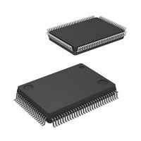
R5F363AENFA#U0 Renesas Electronics America, R5F363AENFA#U0 Datasheet - Page 614

R5F363AENFA#U0
Manufacturer Part Number
R5F363AENFA#U0
Description
MCU 4KB FLASH 256/16K 100-QFP
Manufacturer
Renesas Electronics America
Series
M16C/60/63r
Specifications of R5F363AENFA#U0
Core Processor
M16C/60
Core Size
16/32-Bit
Speed
20MHz
Connectivity
EBI/EMI, I²C, SIO, UART/USART
Peripherals
DMA, LVD, POR, PWM, WDT
Number Of I /o
85
Program Memory Size
256KB (256K x 8)
Program Memory Type
FLASH
Ram Size
20K x 8
Voltage - Supply (vcc/vdd)
1.8 V ~ 5.5 V
Data Converters
A/D 26x10b; D/A 2x8b
Oscillator Type
Internal
Operating Temperature
-20°C ~ 85°C
Package / Case
100-QFP
Lead Free Status / RoHS Status
Lead free / RoHS Compliant
Eeprom Size
-
Available stocks
Company
Part Number
Manufacturer
Quantity
Price
- Current page: 614 of 883
- Download datasheet (13Mb)
M16C/63 Group
REJ09B0510-0100 Rev.1.00 Sep 15, 2009
Page 576 of 836
25.3
25.3.1
Figure 25.5
25.3.1.1
Set the PCKSTP16 bit in the PCLKSTP1 register to 0 (f1 provide enabled).
Figure 25.5 shows the I
f1
m: 2, 4, 8, 2.5, 3, 5, 6
n: 3 to 31 (value set to bits CCR4 to CCR0 in the S20 register)
Note:
1. Set the CPU clock to 100 kHz or lower in standard clock more, and 400 kHz or lower in high-speed clock mode.
fVIIC is determined by setting a combination of the following:
fVIIC stops when the ES0 bit in the S1D0 register is 0 (I
See Table 25.8 “I
Operations
(selectable by bits ICK1 to ICK0 in the S3D0 register and bits ICK4 to ICK2 in the S4D0 register)
•
•
•
•
The frequency of peripheral clock f1
The PCLK0 bit in the PCLKR register
Bits ICK1 to ICK0 in the S3D0 register
Bits ICK4 to ICK2 in the S4D0 register
Clock
I
fVIIC
2
C-bus Interface Clock
Divide-by-2
FASTMODE= 1
S20 register
FASTMODE = 0
2
C-bus System Clock Select Bits” for details.
2
C-bus Interface Clock.
CCR4 to CCR0
f1IIC
f2IIC
≠
= 5
5
PCLKR register
PCLK0 = 1
PCLK0 = 0
Divide-by-8
Divide-by-4
Divide-by-2
fIIC
System clock select
Divide-by-m
2
C interface disabled).
circuit
Divide-by-n
25. Multi-Master I
(1)
I
2
Clock control circuit
C-bus system clock
fVIIC
2
C-bus Interface
Related parts for R5F363AENFA#U0
Image
Part Number
Description
Manufacturer
Datasheet
Request
R

Part Number:
Description:
KIT STARTER FOR M16C/29
Manufacturer:
Renesas Electronics America
Datasheet:

Part Number:
Description:
KIT STARTER FOR R8C/2D
Manufacturer:
Renesas Electronics America
Datasheet:

Part Number:
Description:
R0K33062P STARTER KIT
Manufacturer:
Renesas Electronics America
Datasheet:

Part Number:
Description:
KIT STARTER FOR R8C/23 E8A
Manufacturer:
Renesas Electronics America
Datasheet:

Part Number:
Description:
KIT STARTER FOR R8C/25
Manufacturer:
Renesas Electronics America
Datasheet:

Part Number:
Description:
KIT STARTER H8S2456 SHARPE DSPLY
Manufacturer:
Renesas Electronics America
Datasheet:

Part Number:
Description:
KIT STARTER FOR R8C38C
Manufacturer:
Renesas Electronics America
Datasheet:

Part Number:
Description:
KIT STARTER FOR R8C35C
Manufacturer:
Renesas Electronics America
Datasheet:

Part Number:
Description:
KIT STARTER FOR R8CL3AC+LCD APPS
Manufacturer:
Renesas Electronics America
Datasheet:

Part Number:
Description:
KIT STARTER FOR RX610
Manufacturer:
Renesas Electronics America
Datasheet:

Part Number:
Description:
KIT STARTER FOR R32C/118
Manufacturer:
Renesas Electronics America
Datasheet:

Part Number:
Description:
KIT DEV RSK-R8C/26-29
Manufacturer:
Renesas Electronics America
Datasheet:

Part Number:
Description:
KIT STARTER FOR SH7124
Manufacturer:
Renesas Electronics America
Datasheet:

Part Number:
Description:
KIT STARTER FOR H8SX/1622
Manufacturer:
Renesas Electronics America
Datasheet:

Part Number:
Description:
KIT DEV FOR SH7203
Manufacturer:
Renesas Electronics America
Datasheet:


