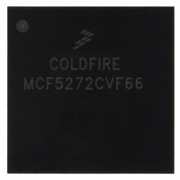
MCF5272CVF66 Freescale Semiconductor, MCF5272CVF66 Datasheet - Page 298

MCF5272CVF66
Manufacturer Part Number
MCF5272CVF66
Description
IC MPU 32BIT 66MHZ 196-MAPBGA
Manufacturer
Freescale Semiconductor
Series
MCF527xr
Specifications of MCF5272CVF66
Core Processor
Coldfire V2
Core Size
32-Bit
Speed
66MHz
Connectivity
EBI/EMI, Ethernet, I²C, SPI, UART/USART, USB
Peripherals
DMA, WDT
Number Of I /o
32
Program Memory Size
16KB (4K x 32)
Program Memory Type
ROM
Ram Size
1K x 32
Voltage - Supply (vcc/vdd)
3 V ~ 3.6 V
Oscillator Type
External
Operating Temperature
-40°C ~ 85°C
Package / Case
196-MAPBGA
Family Name
MCF5xxx
Device Core
ColdFire
Device Core Size
32b
Frequency (max)
66MHz
Instruction Set Architecture
RISC
Supply Voltage 1 (typ)
3.3V
Operating Temp Range
-40C to 85C
Operating Temperature Classification
Industrial
Mounting
Surface Mount
Pin Count
196
Package Type
MA-BGA
Lead Free Status / RoHS Status
Contains lead / RoHS non-compliant
Eeprom Size
-
Data Converters
-
Lead Free Status / Rohs Status
Not Compliant
Available stocks
Company
Part Number
Manufacturer
Quantity
Price
Company:
Part Number:
MCF5272CVF66
Manufacturer:
Freescale Semiconductor
Quantity:
10 000
Part Number:
MCF5272CVF66
Manufacturer:
FREESCALE
Quantity:
20 000
Company:
Part Number:
MCF5272CVF66 K75N
Manufacturer:
ST
Quantity:
18
Company:
Part Number:
MCF5272CVF66J
Manufacturer:
Freescale Semiconductor
Quantity:
10 000
- Current page: 298 of 544
- Download datasheet (7Mb)
Physical Layer Interface Controller (PLIC)
Figure 13-1
The four ports have the following timing and connectivity features:
13-2
•
•
•
•
Pin Set 0
PA8/FSC0/FSR0, PA9/DGNT0,
DCL0/URT1_CLK, DIN0/URT1_RxD,
DOUT0/URT1_TxD, PA10/DREQ0
Port 0: Connects through pin set 0. Operates as a slave-only port; that is, an external device must
source frame sync clock/frame sync receive (FSC/FSR) and data clock (DCL). These pins are
unidirectional inputs. Din0 and Dout0 are dedicated pins for port 0.
Port 1: Connects through pin set 1. Operates as a master or slave port. In slave mode an external
device must source FSC/FSR and DCL. In master mode, DCL1 and FSC1/FSR1 are outputs. These
signals are in turn derived from the DCL0 and FSC/FSR from port 0. For port 1 to function in
master mode, port 0 must be enabled with an external transceiver sourcing DCL and FSC/FSR. The
physical interface pins Din1 and Dout1 serve ports 1, 2, and 3.
Port 2: Connects through pin set 1. Operates as a slave-only port. Port 2 shares a data clock with
port 1: DCL1 when port 1 is in slave mode or GDCL when port 1 is in master mode. A delayed
frame sync, DFSC2, derived from FSC1, is connected to the DFSC2 output and fed to the port 2
IDL/GCI block. Users can synchronize the port 2 IDL/GCI block with an offset frame sync, (offset
with respect to the port 1 GCI/IDL block), by programming the port 2 sync delay register, P2SDR.
Port 3: Connects through pin set 1 or 3. Operates as a slave-only port. Port 3 shares a data clock
with port 1: DCL1 when port 1 is in slave mode, or GDCL, when port 1 is in master mode. A
delayed frame sync, DFSC3, is derived from FSC1 and is fed to the port 3 IDL/GCI block.
Programming the port 3 sync delay register, P3SDR, allows it to be synchronized with an offset
illustrates the basic PLIC system.
GCI/IDL
Port 0
32
MCF5272 ColdFire
Generator
Figure 13-1. PLIC System Diagram
Timing
®
Integrated Microprocessor User’s Manual, Rev. 3
Internal Interface Registers
Pin Set 1
FSC1/FSR1/DFSC1,
DCL1/GDCL1_OUT, PA14,
PA15_INT6/DGNT1_INT6, DOUT1, DIN1
Internal Bus
Timing
Gen
GCI/IDL
Port 1
32
Pin Set 1 Mux
GCI/IDL
Port 2
Timing
Gen
32
Pin Set 3
PA7/QSPI_CS3/DOUT3,
DIN3/INT4
Pin Set 3
GCI/IDL
Port 3
Mux
Freescale Semiconductor
32
DIN3
DOUT
Timing
Gen
Related parts for MCF5272CVF66
Image
Part Number
Description
Manufacturer
Datasheet
Request
R
Part Number:
Description:
Mcf5272 Coldfire Integrated Microprocessor User
Manufacturer:
Freescale Semiconductor, Inc
Datasheet:

Part Number:
Description:
MCF5272 Interrupt Service Routine for the Physical Layer Interface Controller
Manufacturer:
Freescale Semiconductor / Motorola
Datasheet:
Part Number:
Description:
Manufacturer:
Freescale Semiconductor, Inc
Datasheet:
Part Number:
Description:
Manufacturer:
Freescale Semiconductor, Inc
Datasheet:
Part Number:
Description:
Manufacturer:
Freescale Semiconductor, Inc
Datasheet:
Part Number:
Description:
Manufacturer:
Freescale Semiconductor, Inc
Datasheet:
Part Number:
Description:
Manufacturer:
Freescale Semiconductor, Inc
Datasheet:
Part Number:
Description:
Manufacturer:
Freescale Semiconductor, Inc
Datasheet:
Part Number:
Description:
Manufacturer:
Freescale Semiconductor, Inc
Datasheet:
Part Number:
Description:
Manufacturer:
Freescale Semiconductor, Inc
Datasheet:
Part Number:
Description:
Manufacturer:
Freescale Semiconductor, Inc
Datasheet:
Part Number:
Description:
Manufacturer:
Freescale Semiconductor, Inc
Datasheet:
Part Number:
Description:
Manufacturer:
Freescale Semiconductor, Inc
Datasheet:
Part Number:
Description:
Manufacturer:
Freescale Semiconductor, Inc
Datasheet:
Part Number:
Description:
Manufacturer:
Freescale Semiconductor, Inc
Datasheet:


