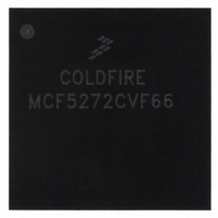
MCF5272CVF66 Freescale Semiconductor, MCF5272CVF66 Datasheet - Page 357

MCF5272CVF66
Manufacturer Part Number
MCF5272CVF66
Description
IC MPU 32BIT 66MHZ 196-MAPBGA
Manufacturer
Freescale Semiconductor
Series
MCF527xr
Specifications of MCF5272CVF66
Core Processor
Coldfire V2
Core Size
32-Bit
Speed
66MHz
Connectivity
EBI/EMI, Ethernet, I²C, SPI, UART/USART, USB
Peripherals
DMA, WDT
Number Of I /o
32
Program Memory Size
16KB (4K x 32)
Program Memory Type
ROM
Ram Size
1K x 32
Voltage - Supply (vcc/vdd)
3 V ~ 3.6 V
Oscillator Type
External
Operating Temperature
-40°C ~ 85°C
Package / Case
196-MAPBGA
Family Name
MCF5xxx
Device Core
ColdFire
Device Core Size
32b
Frequency (max)
66MHz
Instruction Set Architecture
RISC
Supply Voltage 1 (typ)
3.3V
Operating Temp Range
-40C to 85C
Operating Temperature Classification
Industrial
Mounting
Surface Mount
Pin Count
196
Package Type
MA-BGA
Lead Free Status / RoHS Status
Contains lead / RoHS non-compliant
Eeprom Size
-
Data Converters
-
Lead Free Status / Rohs Status
Not Compliant
Available stocks
Company
Part Number
Manufacturer
Quantity
Price
Company:
Part Number:
MCF5272CVF66
Manufacturer:
Freescale Semiconductor
Quantity:
10 000
Part Number:
MCF5272CVF66
Manufacturer:
FREESCALE
Quantity:
20 000
Company:
Part Number:
MCF5272CVF66 K75N
Manufacturer:
ST
Quantity:
18
Company:
Part Number:
MCF5272CVF66J
Manufacturer:
Freescale Semiconductor
Quantity:
10 000
- Current page: 357 of 544
- Download datasheet (7Mb)
15.3
The following sections describe the timer registers.
15.3.1
The TMRs,
TMRn fields are described in
Freescale Semiconductor
15–8
Bits
7–6
2–1
5
4
3
1
Reset
Not implemented (reserved) in TMR2 and TMR3.
Field
Addr
R/W
Name
FRR
CLK
ORI
OM
PS
CE
General-Purpose Timer Registers
15
Timer Mode Registers (TMR0–TMR3)
Table
Prescaler. Programmed to divide the clock input by values from 1 to 256. The value 0000_0000 divides the
clock by 1; the value 1111_1111 divides the clock by 256.
Capture edge and enable interrupt.
00 Disable capture and interrupt on capture event
01 Capture on rising edge only and generate interrupt on capture event
10 Capture on falling edge only and generate interrupt on capture event
11 Capture on any edge and generate interrupt on capture event
Output mode (TMR0 and TMR1 only. Reserved in TMR2 and TMR3)
0 Active-low pulse for one system clock cycle (15 nS at 66 MHz)
1 Toggle output
TOUTn is high at reset but is unavailable externally until the appropriate port control register is configured for
this function. See
Output reference interrupt enable
0 Disable interrupt for reference reached (does not affect interrupt on capture function)
1 Enable interrupt upon reaching the reference value If ORI is 1 when the TER[REF] is set, an immediate
Free run/restart
0 Free run. Timer count continues to increment after the reference value is reached.
1 Restart. Timer count is reset immediately after the reference value is reached.
Input clock source for the timer
00 Stop count
01 Master system clock
10 Master system clock divided by 16. TIN0 and TIN1 are external to the MCF5272 and are not synchronized
11 Corresponding TIN pin, TIN0 or TIN1 (falling edge), unused in TMR2 and TMR3
The minimum high and low periods for TIN as the clock source is 1 system clock, which gives a maximum TIN
frequency of clock/2.
interrupt occurs.
to the system clock, so successive timeout lengths may vary slightly.
15-2, have fields for choosing a prescaler, a clock edge, and other parameters.
MCF5272 ColdFire
PRESCALER (PS)
MBAR + 0x200 (TMR0); 0x220 (TMR1); 0x240 (TMR2); 0x260 (TMR3)
Figure 15-2. Timer Mode Registers (TMR0–TMR3)
Section 17.2, “Port Control
Table
Table 15-1. TMRn Field Descriptions
15-1.
®
Integrated Microprocessor User’s Manual, Rev. 3
0000_0000_0000_0000
Read/Write
Registers.”
8
Description
7
CE
6
OM
5
1
ORI
4
FRR
3
2
CLK
1
Timer Module
RST
0
15-3
Related parts for MCF5272CVF66
Image
Part Number
Description
Manufacturer
Datasheet
Request
R
Part Number:
Description:
Mcf5272 Coldfire Integrated Microprocessor User
Manufacturer:
Freescale Semiconductor, Inc
Datasheet:

Part Number:
Description:
MCF5272 Interrupt Service Routine for the Physical Layer Interface Controller
Manufacturer:
Freescale Semiconductor / Motorola
Datasheet:
Part Number:
Description:
Manufacturer:
Freescale Semiconductor, Inc
Datasheet:
Part Number:
Description:
Manufacturer:
Freescale Semiconductor, Inc
Datasheet:
Part Number:
Description:
Manufacturer:
Freescale Semiconductor, Inc
Datasheet:
Part Number:
Description:
Manufacturer:
Freescale Semiconductor, Inc
Datasheet:
Part Number:
Description:
Manufacturer:
Freescale Semiconductor, Inc
Datasheet:
Part Number:
Description:
Manufacturer:
Freescale Semiconductor, Inc
Datasheet:
Part Number:
Description:
Manufacturer:
Freescale Semiconductor, Inc
Datasheet:
Part Number:
Description:
Manufacturer:
Freescale Semiconductor, Inc
Datasheet:
Part Number:
Description:
Manufacturer:
Freescale Semiconductor, Inc
Datasheet:
Part Number:
Description:
Manufacturer:
Freescale Semiconductor, Inc
Datasheet:
Part Number:
Description:
Manufacturer:
Freescale Semiconductor, Inc
Datasheet:
Part Number:
Description:
Manufacturer:
Freescale Semiconductor, Inc
Datasheet:
Part Number:
Description:
Manufacturer:
Freescale Semiconductor, Inc
Datasheet:


