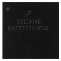
MCF5272CVF66 Freescale Semiconductor, MCF5272CVF66 Datasheet - Page 440

MCF5272CVF66
Manufacturer Part Number
MCF5272CVF66
Description
IC MPU 32BIT 66MHZ 196-MAPBGA
Manufacturer
Freescale Semiconductor
Series
MCF527xr
Specifications of MCF5272CVF66
Core Processor
Coldfire V2
Core Size
32-Bit
Speed
66MHz
Connectivity
EBI/EMI, Ethernet, I²C, SPI, UART/USART, USB
Peripherals
DMA, WDT
Number Of I /o
32
Program Memory Size
16KB (4K x 32)
Program Memory Type
ROM
Ram Size
1K x 32
Voltage - Supply (vcc/vdd)
3 V ~ 3.6 V
Oscillator Type
External
Operating Temperature
-40°C ~ 85°C
Package / Case
196-MAPBGA
Family Name
MCF5xxx
Device Core
ColdFire
Device Core Size
32b
Frequency (max)
66MHz
Instruction Set Architecture
RISC
Supply Voltage 1 (typ)
3.3V
Operating Temp Range
-40C to 85C
Operating Temperature Classification
Industrial
Mounting
Surface Mount
Pin Count
196
Package Type
MA-BGA
Lead Free Status / RoHS Status
Contains lead / RoHS non-compliant
Eeprom Size
-
Data Converters
-
Lead Free Status / Rohs Status
Not Compliant
Available stocks
Company
Part Number
Manufacturer
Quantity
Price
Company:
Part Number:
MCF5272CVF66
Manufacturer:
Freescale Semiconductor
Quantity:
10 000
Part Number:
MCF5272CVF66
Manufacturer:
FREESCALE
Quantity:
20 000
Company:
Part Number:
MCF5272CVF66 K75N
Manufacturer:
ST
Quantity:
18
Company:
Part Number:
MCF5272CVF66J
Manufacturer:
Freescale Semiconductor
Quantity:
10 000
- Current page: 440 of 544
- Download datasheet (7Mb)
Signal Descriptions
19.15.1 QSPI Synchronous Serial Data Output (QSPI_Dout/WSEL)
The QSPI synchronous serial data output (QSPI_Dout) can be programmed to be driven on the rising or
falling edge of SCK. Each byte is sent msb first.
WSEL configuration input is sampled on the rising edge of Reset Output (RSTO).
19.15.2 QSPI Synchronous Serial Data Input (QSPI_Din)
The QSPI synchronous serial data input (QSPI_Din) can be programmed to be sampled on the rising or
falling edge of QSPI_CLK. Each byte is written to RAM lsb first.
19.15.3 QSPI Serial Clock (QSPI_CLK/BUSW1)
The QSPI serial clock (QSPI_CLK/BUSW1) provides the serial clock from the QSPI. The polarity and
phase of QSPI_CLK are programmable. The output frequency is programmed according to the following
formula, in which n can be any value between 1 and 255:
At reset, QSPI_CLK/BUSW1 is used to configure the width of memory connected to CS0.
BUSW1 configuration input is sampled on the rising edge of Reset Output (RSTO).
19.15.4 Synchronous Peripheral Chip Select 0 (QSPI_CS0/BUSW0)
The synchronous peripheral chip select 0 (QSPI_CS0) output provides a QSPI peripheral chip select that
can be programmed to be active high or low. During reset, this pin is used to configure the width of
memory connected to CS0.
BUSW0 configuration input is sampled on the rising edge of Reset Output (RSTO).
19.15.5 Synchronous Peripheral Chip Select 1 (QSPI_CS1/PA11)
See
QSPI_CS1 can be programmed to be active high or low.
19.15.6 Synchronous Peripheral Chip Select 2 (QSPI_CS2/URT1_CTS)
See
19.15.7 Synchronous Peripheral Chip Select 3 (PA7/DOUT3/QSPI_CS3)
See
description for GPIO ports.
19-30
Section 19.16.1.9, “QSPI Chip Select 1
Section 19.16.1.5, “UART1 CTS
Section 19.16.3.3, “QSPI_CS3, Port 3 GCI/IDL Data Out 3, PA7
QSPI_CLK = CLKIN/(2 × n)
MCF5272 ColdFire
(URT1_CTS/QSPI_CS2).”
®
Integrated Microprocessor User’s Manual, Rev. 3
(QSPI_CS1/PA11).”
(PA7/DOUT3/QSPI_CS3).” See
Freescale Semiconductor
Related parts for MCF5272CVF66
Image
Part Number
Description
Manufacturer
Datasheet
Request
R
Part Number:
Description:
Mcf5272 Coldfire Integrated Microprocessor User
Manufacturer:
Freescale Semiconductor, Inc
Datasheet:

Part Number:
Description:
MCF5272 Interrupt Service Routine for the Physical Layer Interface Controller
Manufacturer:
Freescale Semiconductor / Motorola
Datasheet:
Part Number:
Description:
Manufacturer:
Freescale Semiconductor, Inc
Datasheet:
Part Number:
Description:
Manufacturer:
Freescale Semiconductor, Inc
Datasheet:
Part Number:
Description:
Manufacturer:
Freescale Semiconductor, Inc
Datasheet:
Part Number:
Description:
Manufacturer:
Freescale Semiconductor, Inc
Datasheet:
Part Number:
Description:
Manufacturer:
Freescale Semiconductor, Inc
Datasheet:
Part Number:
Description:
Manufacturer:
Freescale Semiconductor, Inc
Datasheet:
Part Number:
Description:
Manufacturer:
Freescale Semiconductor, Inc
Datasheet:
Part Number:
Description:
Manufacturer:
Freescale Semiconductor, Inc
Datasheet:
Part Number:
Description:
Manufacturer:
Freescale Semiconductor, Inc
Datasheet:
Part Number:
Description:
Manufacturer:
Freescale Semiconductor, Inc
Datasheet:
Part Number:
Description:
Manufacturer:
Freescale Semiconductor, Inc
Datasheet:
Part Number:
Description:
Manufacturer:
Freescale Semiconductor, Inc
Datasheet:
Part Number:
Description:
Manufacturer:
Freescale Semiconductor, Inc
Datasheet:


