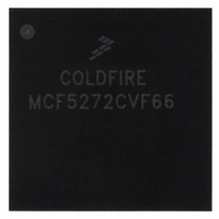
MCF5272CVF66 Freescale Semiconductor, MCF5272CVF66 Datasheet - Page 337

MCF5272CVF66
Manufacturer Part Number
MCF5272CVF66
Description
IC MPU 32BIT 66MHZ 196-MAPBGA
Manufacturer
Freescale Semiconductor
Series
MCF527xr
Specifications of MCF5272CVF66
Core Processor
Coldfire V2
Core Size
32-Bit
Speed
66MHz
Connectivity
EBI/EMI, Ethernet, I²C, SPI, UART/USART, USB
Peripherals
DMA, WDT
Number Of I /o
32
Program Memory Size
16KB (4K x 32)
Program Memory Type
ROM
Ram Size
1K x 32
Voltage - Supply (vcc/vdd)
3 V ~ 3.6 V
Oscillator Type
External
Operating Temperature
-40°C ~ 85°C
Package / Case
196-MAPBGA
Family Name
MCF5xxx
Device Core
ColdFire
Device Core Size
32b
Frequency (max)
66MHz
Instruction Set Architecture
RISC
Supply Voltage 1 (typ)
3.3V
Operating Temp Range
-40C to 85C
Operating Temperature Classification
Industrial
Mounting
Surface Mount
Pin Count
196
Package Type
MA-BGA
Lead Free Status / RoHS Status
Contains lead / RoHS non-compliant
Eeprom Size
-
Data Converters
-
Lead Free Status / Rohs Status
Not Compliant
Available stocks
Company
Part Number
Manufacturer
Quantity
Price
Company:
Part Number:
MCF5272CVF66
Manufacturer:
Freescale Semiconductor
Quantity:
10 000
Part Number:
MCF5272CVF66
Manufacturer:
FREESCALE
Quantity:
20 000
Company:
Part Number:
MCF5272CVF66 K75N
Manufacturer:
ST
Quantity:
18
Company:
Part Number:
MCF5272CVF66J
Manufacturer:
Freescale Semiconductor
Quantity:
10 000
- Current page: 337 of 544
- Download datasheet (7Mb)
In the above example, CODEC 1 transmits and receives in the B3 time slot once the U transceiver has
completed the D channel. From the rising edge of FSC1, this is at least 19 DCL clocks later. In
Figure
channel. For example, let us say this is 1 DCL clocks long. This defines the programmable delay 1 value
to be 20, (19 + 1), or 0x0014. The DFSC3 signal synchronizes CODECs 3 and 4, and the rising edge of
this frame sync occurs 20 clocks after DFSC2, therefore 40 DCL clocks after FSC1. This defines the value
for programmable delay 3 to be 40, (19 + 1 + 20), or 0x0028.
13.6.5
In this example, ports 0 and 1 are connected to two S/T transceivers. Ports 0 and 1 are programmed in
slave mode. Ports 2 and 3 are not used, and may be disabled.
Freescale Semiconductor
DFSC2
DFSC3
Dout1
FSC1
Din1/
DCL
13-40, a short, optional delay, is shown between the end of the D channel and the start of the B3
Example 3: Two-Line Remote Access with Ports 0 and 1
B1
U Transceiver
MCF5272 ColdFire
MCF5272
D
Interface 1
Interface 0
B2
Figure 13-40. Standard IDL2 10-Bit Mode
Figure 13-41. Two-Line Remote Access
DREQ1
DREQ0
DGNT1
DGNT0
®
Dout1
Dout0
FSC1
DCL1
FSC0
DCL0
D
Din1
Integrated Microprocessor User’s Manual, Rev. 3
Din0
CODEC 1
B3
CODEC 2
B4
Tx
IDL SYNC
Tx
Rx
IDL SYNC
Rx
DGrant
IDL CLK
DGrant
DRequest
IDL CLK
DRequest
MC145574 #1
MC145574 #2
Physical Layer Interface Controller (PLIC)
CODEC 3
B5
CODEC 4
B6
13-41
Related parts for MCF5272CVF66
Image
Part Number
Description
Manufacturer
Datasheet
Request
R
Part Number:
Description:
Mcf5272 Coldfire Integrated Microprocessor User
Manufacturer:
Freescale Semiconductor, Inc
Datasheet:

Part Number:
Description:
MCF5272 Interrupt Service Routine for the Physical Layer Interface Controller
Manufacturer:
Freescale Semiconductor / Motorola
Datasheet:
Part Number:
Description:
Manufacturer:
Freescale Semiconductor, Inc
Datasheet:
Part Number:
Description:
Manufacturer:
Freescale Semiconductor, Inc
Datasheet:
Part Number:
Description:
Manufacturer:
Freescale Semiconductor, Inc
Datasheet:
Part Number:
Description:
Manufacturer:
Freescale Semiconductor, Inc
Datasheet:
Part Number:
Description:
Manufacturer:
Freescale Semiconductor, Inc
Datasheet:
Part Number:
Description:
Manufacturer:
Freescale Semiconductor, Inc
Datasheet:
Part Number:
Description:
Manufacturer:
Freescale Semiconductor, Inc
Datasheet:
Part Number:
Description:
Manufacturer:
Freescale Semiconductor, Inc
Datasheet:
Part Number:
Description:
Manufacturer:
Freescale Semiconductor, Inc
Datasheet:
Part Number:
Description:
Manufacturer:
Freescale Semiconductor, Inc
Datasheet:
Part Number:
Description:
Manufacturer:
Freescale Semiconductor, Inc
Datasheet:
Part Number:
Description:
Manufacturer:
Freescale Semiconductor, Inc
Datasheet:
Part Number:
Description:
Manufacturer:
Freescale Semiconductor, Inc
Datasheet:


