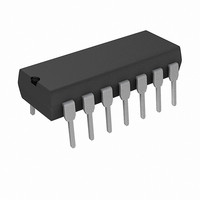
PIC16F1824-I/P Microchip Technology, PIC16F1824-I/P Datasheet - Page 217

PIC16F1824-I/P
Manufacturer Part Number
PIC16F1824-I/P
Description
IC PIC MCU 8BIT 14KB FLSH 14PDIP
Manufacturer
Microchip Technology
Series
PIC® XLP™ 16Fr
Datasheets
1.PIC16F722-ISS.pdf
(8 pages)
2.PIC16F1824-ISL.pdf
(2 pages)
3.PIC16F1824-ISL.pdf
(419 pages)
4.PIC16F1824-ISL.pdf
(10 pages)
5.PIC16F1824-IP.pdf
(10 pages)
Specifications of PIC16F1824-I/P
Core Processor
PIC
Core Size
8-Bit
Speed
32MHz
Connectivity
I²C, SPI, UART/USART
Peripherals
Brown-out Detect/Reset, POR, PWM, WDT
Number Of I /o
11
Program Memory Size
7KB (4K x 14)
Program Memory Type
FLASH
Eeprom Size
256 x 8
Ram Size
256 x 8
Voltage - Supply (vcc/vdd)
1.8 V ~ 5.5 V
Data Converters
A/D 8x10b
Oscillator Type
Internal
Operating Temperature
-40°C ~ 85°C
Package / Case
14-DIP (0.300", 7.62mm)
Processor Series
PIC16F
Core
PIC
3rd Party Development Tools
52715-96, 52716-328, 52717-734
Development Tools By Supplier
PG164130, DV164035, DV244005, DV164005
Lead Free Status / RoHS Status
Lead free / RoHS Compliant
Lead Free Status / RoHS Status
Lead free / RoHS Compliant, Lead free / RoHS Compliant
- PIC16F722-ISS PDF datasheet
- PIC16F1824-ISL PDF datasheet #2
- PIC16F1824-ISL PDF datasheet #3
- PIC16F1824-ISL PDF datasheet #4
- PIC16F1824-IP PDF datasheet #5
- Current page: 217 of 419
- Download datasheet (4Mb)
24.1.5
Capture mode depends upon the Timer1 module for
proper operation. There are two options for driving the
Timer1 module in Capture mode. It can be driven by the
instruction clock (F
When Timer1 is clocked by F
increment during Sleep. When the device wakes from
Sleep, Timer1 will continue from its previous state.
Capture mode will operate during Sleep when Timer1
is clocked by an external clock source.
TABLE 24-2:
2010 Microchip Technology Inc.
APFCON1
CCPxCON
CCPRxL
CCPRxH
CMxCON0
CMxCON1
INLVLA
INLVLC
INTCON
PIE1
PIE2
PIE3
PIR1
PIR2
PIR3
T1CON
T1GCON
TMR1L
TMR1H
TRISA
TRISC
Legend: — = Unimplemented locations, read as ‘0’. Shaded cells are not used by the Capture.
Note 1:
Name
2:
*
Page provides register information.
Applies to ECCP modules only.
PIC16F/LF1828 only.
CAPTURE DURING SLEEP
Capture/Compare/PWM Register x Low Byte (LSB)
Capture/Compare/PWM Register x High Byte (MSB)
Holding Register for the Least Significant Byte of the 16-bit TMR1 Register
Holding Register for the Most Significant Byte of the 16-bit TMR1 Register
INLVLC7
TMR1CS1 TMR1CS0 T1CKPS1
TRISC7
TMR1GIE
TMR1GIF
TMR1GE
PxM1
CxINTP
OSFIE
OSFIF
CxON
Bit 7
GIE
—
—
—
—
—
OSC
SUMMARY OF REGISTERS ASSOCIATED WITH CAPTURE
(1)
(2)
(2)
/4), or by an external clock source.
INLVLC6
TRISC6
T1GPOL
PxM0
CxINTN
CxOUT
PEIE
ADIE
C2IE
ADIF
Bit 6
C2IF
—
—
—
—
—
(1)
OSC
(2)
(2)
/4, Timer1 will not
INLVLC5
CxPCH1
INLVLA5
TMR0IE
CCP4IE
CCP4IF
TRISC5
TRISA5
T1GTM
DCxB1
CxOE
RCIE
RCIF
C1IE
Bit 5
C1IF
—
T1CKPS0
INLVLC4
T1GSPM
CxPCH0
INLVLA4
CCP3IE
CCP3IF
TRISA4
TRISC4
CxPOL
DCxB0
INTE
EEIE
Bit 4
TXIE
TXIF
EEIF
—
Preliminary
T1GGO/DONE
T1OSCEN
CCPxM3
INLVLC3
P1DSEL
INLVLA3
TMR6IE
SSP1IE
TMR6IF
TRISA3
TRISC3
BCL1IE
SSP1IF
BCL1IF
IOCIE
Bit 3
24.1.6
This module incorporates I/O pins that can be moved to
other locations with the use of the alternate pin function
registers, APFCON0 and APFCON1. To determine
which pins can be moved and what their default loca-
tions are upon a Reset, see
Pin Function”
—
—
PIC16(L)F1824/1828
CCPxM2
INLVLC2
P1CSEL
INLVLA2
T1SYNC
T1GVAL
TMR0IF
CCP1IE
CCP1IF
TRISC2
TRISA2
ALTERNATE PIN LOCATIONS
CxSP
Bit 2
—
—
—
—
—
for more information.
CCPxM1
CxNCH1
INLVLA1
INLVLC1
P2BSEL
T1GSS1
TMR2IE
TMR4IE
TMR2IF
TMR4IF
TRISC1
TRISA1
CxHYS
INTF
Bit 1
—
—
—
Section 12.1 “Alternate
CCP2SEL
TMR1ON
CCPxM0
CxSYNC
CxNCH0
INLVLA0
INLVLC0
T1GSS0
TMR1IE
CCP2IE
TMR1IF
CCP2IF
TRISA0
TRISC0
IOCIF
Bit 0
DS41419B-page 217
—
—
Register
on Page
216*
216*
193*
193*
123
238
181
182
128
139
197
198
126
137
93
94
95
96
97
98
99
Related parts for PIC16F1824-I/P
Image
Part Number
Description
Manufacturer
Datasheet
Request
R

Part Number:
Description:
IC, 8BIT MCU, PIC16F, 32MHZ, SOIC-18
Manufacturer:
Microchip Technology
Datasheet:

Part Number:
Description:
IC, 8BIT MCU, PIC16F, 32MHZ, SSOP-20
Manufacturer:
Microchip Technology
Datasheet:

Part Number:
Description:
IC, 8BIT MCU, PIC16F, 32MHZ, DIP-18
Manufacturer:
Microchip Technology
Datasheet:

Part Number:
Description:
IC, 8BIT MCU, PIC16F, 32MHZ, QFN-28
Manufacturer:
Microchip Technology
Datasheet:

Part Number:
Description:
IC, 8BIT MCU, PIC16F, 32MHZ, QFN-28
Manufacturer:
Microchip Technology
Datasheet:

Part Number:
Description:
IC, 8BIT MCU, PIC16F, 32MHZ, QFN-28
Manufacturer:
Microchip Technology
Datasheet:

Part Number:
Description:
IC, 8BIT MCU, PIC16F, 32MHZ, SSOP-20
Manufacturer:
Microchip Technology
Datasheet:

Part Number:
Description:
IC, 8BIT MCU, PIC16F, 20MHZ, DIP-40
Manufacturer:
Microchip Technology
Datasheet:

Part Number:
Description:
IC, 8BIT MCU, PIC16F, 32MHZ, QFN-28
Manufacturer:
Microchip Technology
Datasheet:

Part Number:
Description:
IC, 8BIT MCU, PIC16F, 20MHZ, MQFP-44
Manufacturer:
Microchip Technology
Datasheet:

Part Number:
Description:
IC, 8BIT MCU, PIC16F, 20MHZ, QFN-20
Manufacturer:
Microchip Technology
Datasheet:

Part Number:
Description:
IC, 8BIT MCU, PIC16F, 32MHZ, QFN-28
Manufacturer:
Microchip Technology
Datasheet:

Part Number:
Description:
MCU 14KB FLASH 768B RAM 64-TQFP
Manufacturer:
Microchip Technology
Datasheet:

Part Number:
Description:
7 KB Flash, 384 Bytes RAM, 32 MHz Int. Osc, 16 I/0, Enhanced Mid Range Core, Low
Manufacturer:
Microchip Technology

Part Number:
Description:
14KB Flash, 512B RAM, 256B EEPROM, LCD, 1.8-5.5V 40 UQFN 5x5x0.5mm TUBE
Manufacturer:
Microchip Technology
Datasheet:


