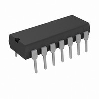
PIC16F1824-I/P Microchip Technology, PIC16F1824-I/P Datasheet - Page 324

PIC16F1824-I/P
Manufacturer Part Number
PIC16F1824-I/P
Description
IC PIC MCU 8BIT 14KB FLSH 14PDIP
Manufacturer
Microchip Technology
Series
PIC® XLP™ 16Fr
Datasheets
1.PIC16F722-ISS.pdf
(8 pages)
2.PIC16F1824-ISL.pdf
(2 pages)
3.PIC16F1824-ISL.pdf
(419 pages)
4.PIC16F1824-ISL.pdf
(10 pages)
5.PIC16F1824-IP.pdf
(10 pages)
Specifications of PIC16F1824-I/P
Core Processor
PIC
Core Size
8-Bit
Speed
32MHz
Connectivity
I²C, SPI, UART/USART
Peripherals
Brown-out Detect/Reset, POR, PWM, WDT
Number Of I /o
11
Program Memory Size
7KB (4K x 14)
Program Memory Type
FLASH
Eeprom Size
256 x 8
Ram Size
256 x 8
Voltage - Supply (vcc/vdd)
1.8 V ~ 5.5 V
Data Converters
A/D 8x10b
Oscillator Type
Internal
Operating Temperature
-40°C ~ 85°C
Package / Case
14-DIP (0.300", 7.62mm)
Processor Series
PIC16F
Core
PIC
3rd Party Development Tools
52715-96, 52716-328, 52717-734
Development Tools By Supplier
PG164130, DV164035, DV244005, DV164005
Lead Free Status / RoHS Status
Lead free / RoHS Compliant
Lead Free Status / RoHS Status
Lead free / RoHS Compliant, Lead free / RoHS Compliant
- PIC16F722-ISS PDF datasheet
- PIC16F1824-ISL PDF datasheet #2
- PIC16F1824-ISL PDF datasheet #3
- PIC16F1824-ISL PDF datasheet #4
- PIC16F1824-IP PDF datasheet #5
- Current page: 324 of 419
- Download datasheet (4Mb)
26.4.2.3
The operation of the Synchronous Master and Slave
modes is identical
Master
• Sleep
• CREN bit is always set, therefore the receiver is
• SREN bit, which is a “don’t care” in Slave mode
A character may be received while in Sleep mode by
setting the CREN bit prior to entering Sleep. Once the
word is received, the RSR register will transfer the data
to the RCREG register. If the RCIE enable bit is set, the
interrupt generated will wake the device from Sleep
and execute the next instruction. If the GIE bit is also
set, the program will branch to the interrupt vector.
TABLE 26-10: SUMMARY OF REGISTERS ASSOCIATED WITH SYNCHRONOUS SLAVE
2010 Microchip Technology Inc.
APFCON0
BAUDCON
INTCON
PIE1
PIR1
RCREG
RCSTA
TXSTA
Legend:
Note 1:
never Idle
Name
Reception”), with the following exceptions:
*
— = unimplemented location, read as ‘0’. Shaded cells are not used for Synchronous Slave Reception.
Page provides register information.
PIC16F/LF1824 only.
EUSART Synchronous Slave
Reception
RXDTSEL
TMR1GIE
TMR1GIF
ABDOVF
CSRC
SPEN
RECEPTION
Bit 7
GIE
(Section 26.4.1.5 “Synchronous
SDOSEL
RCIDL
PEIE
ADIE
ADIF
Bit 6
RX9
TX9
(1)
SSSEL
TMR0IE
SREN
TXEN
RCIE
RCIF
Bit 5
—
EUSART Receive Data Register
(1)
Preliminary
SCKP
CREN
SYNC
INTE
Bit 4
TXIE
TXIF
—
T1GSEL
SSP1IE
SSP1IF
ADDEN
SENDB
BRG16
26.4.2.4
1.
2.
3.
4.
5.
6.
7.
8.
9.
IOCIE
Bit 3
PIC16(L)F1824/1828
Set the SYNC and SPEN bits and clear the
CSRC bit.
Clear the ANSEL bit for both the CK and DT pins
(if applicable).
If interrupts are desired, set the RCIE bit of the
PIE1 register and the GIE and PEIE bits of the
INTCON register.
If 9-bit reception is desired, set the RX9 bit.
Set the CREN bit to enable reception.
The RCIF bit will be set when reception is
complete. An interrupt will be generated if the
RCIE bit was set.
If 9-bit mode is enabled, retrieve the Most
Significant bit from the RX9D bit of the RCSTA
register.
Retrieve the 8 Least Significant bits from the
receive FIFO by reading the RCREG register.
If an overrun error occurs, clear the error by
either clearing the CREN bit of the RCSTA
register or by clearing the SPEN bit which resets
the EUSART.
TXCKSEL
TMR0IF
CCP1IE
CCP1IF
BRGH
FERR
Bit 2
—
Synchronous Slave Reception
Setup:
TMR2IE
TMR2IF
OERR
TRMT
WUE
Bit 1
INTF
—
TMR1IE
TMR1IF
ABDEN
IOCIF
RX9D
TX9D
Bit 0
DS41419B-page 323
—
Register
on Page
302*
122
308
307
306
93
94
97
Related parts for PIC16F1824-I/P
Image
Part Number
Description
Manufacturer
Datasheet
Request
R

Part Number:
Description:
IC, 8BIT MCU, PIC16F, 32MHZ, SOIC-18
Manufacturer:
Microchip Technology
Datasheet:

Part Number:
Description:
IC, 8BIT MCU, PIC16F, 32MHZ, SSOP-20
Manufacturer:
Microchip Technology
Datasheet:

Part Number:
Description:
IC, 8BIT MCU, PIC16F, 32MHZ, DIP-18
Manufacturer:
Microchip Technology
Datasheet:

Part Number:
Description:
IC, 8BIT MCU, PIC16F, 32MHZ, QFN-28
Manufacturer:
Microchip Technology
Datasheet:

Part Number:
Description:
IC, 8BIT MCU, PIC16F, 32MHZ, QFN-28
Manufacturer:
Microchip Technology
Datasheet:

Part Number:
Description:
IC, 8BIT MCU, PIC16F, 32MHZ, QFN-28
Manufacturer:
Microchip Technology
Datasheet:

Part Number:
Description:
IC, 8BIT MCU, PIC16F, 32MHZ, SSOP-20
Manufacturer:
Microchip Technology
Datasheet:

Part Number:
Description:
IC, 8BIT MCU, PIC16F, 20MHZ, DIP-40
Manufacturer:
Microchip Technology
Datasheet:

Part Number:
Description:
IC, 8BIT MCU, PIC16F, 32MHZ, QFN-28
Manufacturer:
Microchip Technology
Datasheet:

Part Number:
Description:
IC, 8BIT MCU, PIC16F, 20MHZ, MQFP-44
Manufacturer:
Microchip Technology
Datasheet:

Part Number:
Description:
IC, 8BIT MCU, PIC16F, 20MHZ, QFN-20
Manufacturer:
Microchip Technology
Datasheet:

Part Number:
Description:
IC, 8BIT MCU, PIC16F, 32MHZ, QFN-28
Manufacturer:
Microchip Technology
Datasheet:

Part Number:
Description:
MCU 14KB FLASH 768B RAM 64-TQFP
Manufacturer:
Microchip Technology
Datasheet:

Part Number:
Description:
7 KB Flash, 384 Bytes RAM, 32 MHz Int. Osc, 16 I/0, Enhanced Mid Range Core, Low
Manufacturer:
Microchip Technology

Part Number:
Description:
14KB Flash, 512B RAM, 256B EEPROM, LCD, 1.8-5.5V 40 UQFN 5x5x0.5mm TUBE
Manufacturer:
Microchip Technology
Datasheet:


