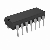
PIC16F1824-I/P Microchip Technology, PIC16F1824-I/P Datasheet - Page 27

PIC16F1824-I/P
Manufacturer Part Number
PIC16F1824-I/P
Description
IC PIC MCU 8BIT 14KB FLSH 14PDIP
Manufacturer
Microchip Technology
Series
PIC® XLP™ 16Fr
Datasheets
1.PIC16F722-ISS.pdf
(8 pages)
2.PIC16F1824-ISL.pdf
(2 pages)
3.PIC16F1824-ISL.pdf
(419 pages)
4.PIC16F1824-ISL.pdf
(10 pages)
5.PIC16F1824-IP.pdf
(10 pages)
Specifications of PIC16F1824-I/P
Core Processor
PIC
Core Size
8-Bit
Speed
32MHz
Connectivity
I²C, SPI, UART/USART
Peripherals
Brown-out Detect/Reset, POR, PWM, WDT
Number Of I /o
11
Program Memory Size
7KB (4K x 14)
Program Memory Type
FLASH
Eeprom Size
256 x 8
Ram Size
256 x 8
Voltage - Supply (vcc/vdd)
1.8 V ~ 5.5 V
Data Converters
A/D 8x10b
Oscillator Type
Internal
Operating Temperature
-40°C ~ 85°C
Package / Case
14-DIP (0.300", 7.62mm)
Processor Series
PIC16F
Core
PIC
3rd Party Development Tools
52715-96, 52716-328, 52717-734
Development Tools By Supplier
PG164130, DV164035, DV244005, DV164005
Lead Free Status / RoHS Status
Lead free / RoHS Compliant
Lead Free Status / RoHS Status
Lead free / RoHS Compliant, Lead free / RoHS Compliant
- PIC16F722-ISS PDF datasheet
- PIC16F1824-ISL PDF datasheet #2
- PIC16F1824-ISL PDF datasheet #3
- PIC16F1824-ISL PDF datasheet #4
- PIC16F1824-IP PDF datasheet #5
- Current page: 27 of 419
- Download datasheet (4Mb)
3.2.2
The Special Function Registers are registers used by
the application to control the desired operation of
peripheral functions in the device. The registers asso-
ciated with the operation of the peripherals are
described in the appropriate peripheral chapter of this
data sheet.
3.2.3
There are up to 80 bytes of GPR in each data memory
bank.
3.2.3.1
The general purpose RAM can be accessed in a
non-banked method via the FSRs. This can simplify
access to large memory structures. See
“Linear Data Memory”
3.2.4
There are 16 bytes of common RAM accessible from all
banks.
FIGURE 3-2:
2010 Microchip Technology Inc.
7-bit Bank Offset
SPECIAL FUNCTION REGISTER
GENERAL PURPOSE RAM
COMMON RAM
Linear Access to GPR
0Ch
0Bh
1Fh
6Fh
7Fh
00h
20h
70h
Special Function Registers
BANKED MEMORY
PARTITIONING
General Purpose RAM
(20 bytes maximum)
(80 bytes maximum)
for more information.
Memory Region
Core Registers
Common RAM
(12 bytes)
(16 bytes)
Section 3.5.2
Preliminary
3.2.5
The memory maps for the device family are as shown
in
TABLE 3-2:
PIC16(L)F1824/1828
Table
PIC16F/LF1824/1828
3-2.
Device
DEVICE MEMORY MAPS
MEMORY MAP TABLES
Banks
16-23
24-31
8-15
0-7
31
DS41419B-page 27
Table No.
Table 3-3
Table 3-4
Table 3-5
Table 3-6
Table 3-7
Related parts for PIC16F1824-I/P
Image
Part Number
Description
Manufacturer
Datasheet
Request
R

Part Number:
Description:
IC, 8BIT MCU, PIC16F, 32MHZ, SOIC-18
Manufacturer:
Microchip Technology
Datasheet:

Part Number:
Description:
IC, 8BIT MCU, PIC16F, 32MHZ, SSOP-20
Manufacturer:
Microchip Technology
Datasheet:

Part Number:
Description:
IC, 8BIT MCU, PIC16F, 32MHZ, DIP-18
Manufacturer:
Microchip Technology
Datasheet:

Part Number:
Description:
IC, 8BIT MCU, PIC16F, 32MHZ, QFN-28
Manufacturer:
Microchip Technology
Datasheet:

Part Number:
Description:
IC, 8BIT MCU, PIC16F, 32MHZ, QFN-28
Manufacturer:
Microchip Technology
Datasheet:

Part Number:
Description:
IC, 8BIT MCU, PIC16F, 32MHZ, QFN-28
Manufacturer:
Microchip Technology
Datasheet:

Part Number:
Description:
IC, 8BIT MCU, PIC16F, 32MHZ, SSOP-20
Manufacturer:
Microchip Technology
Datasheet:

Part Number:
Description:
IC, 8BIT MCU, PIC16F, 20MHZ, DIP-40
Manufacturer:
Microchip Technology
Datasheet:

Part Number:
Description:
IC, 8BIT MCU, PIC16F, 32MHZ, QFN-28
Manufacturer:
Microchip Technology
Datasheet:

Part Number:
Description:
IC, 8BIT MCU, PIC16F, 20MHZ, MQFP-44
Manufacturer:
Microchip Technology
Datasheet:

Part Number:
Description:
IC, 8BIT MCU, PIC16F, 20MHZ, QFN-20
Manufacturer:
Microchip Technology
Datasheet:

Part Number:
Description:
IC, 8BIT MCU, PIC16F, 32MHZ, QFN-28
Manufacturer:
Microchip Technology
Datasheet:

Part Number:
Description:
MCU 14KB FLASH 768B RAM 64-TQFP
Manufacturer:
Microchip Technology
Datasheet:

Part Number:
Description:
7 KB Flash, 384 Bytes RAM, 32 MHz Int. Osc, 16 I/0, Enhanced Mid Range Core, Low
Manufacturer:
Microchip Technology

Part Number:
Description:
14KB Flash, 512B RAM, 256B EEPROM, LCD, 1.8-5.5V 40 UQFN 5x5x0.5mm TUBE
Manufacturer:
Microchip Technology
Datasheet:


