PIC14000-04I/SS Microchip Technology, PIC14000-04I/SS Datasheet - Page 145
PIC14000-04I/SS
Manufacturer Part Number
PIC14000-04I/SS
Description
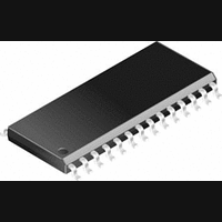
IC, 8BIT MCU, PIC14, 4MHZ, SSOP-28
Manufacturer
Microchip Technology
Datasheet
1.PIC14000-04SO.pdf
(153 pages)
Specifications of PIC14000-04I/SS
Controller Family/series
PIC14
No. Of I/o's
22
Ram Memory Size
192Byte
Cpu Speed
4MHz
No. Of Timers
2
Interface
I2C
Digital Ic Case Style
SSOP
Core Size
8 Bit
Program Memory Size
4096 X 14
Embedded Interface Type
I2C
Rohs Compliant
Yes
Processor Series
PIC14000
Core
PIC
Data Bus Width
8 bit
Program Memory Type
EPROM
Data Ram Size
192 B
Interface Type
SPI, UART
Maximum Clock Frequency
20 MHz
Number Of Programmable I/os
22
Number Of Timers
1
Operating Supply Voltage
2.7 V to 6 V
Maximum Operating Temperature
+ 85 C
Mounting Style
SMD/SMT
Package / Case
SSOP-28
Development Tools By Supplier
ICE2000
Minimum Operating Temperature
- 40 C
On-chip Adc
14 bit
Lead Free Status / RoHS Status
Lead free / RoHS Compliant


Figure 7-15:
Figure 7-16:
Figure 7-17:
Figure 7-18:
Figure 8-1:
Figure 8-2:
Figure 8-3:
Figure 8-4:
Figure 8-5:
Figure 8-6:
Figure 9-1:
Figure 9-2:
Figure 9-3:
Figure 9-4:
Figure 9-5:
Figure 9-6:
Figure 9-7:
Figure 9-8:
Figure 10-1:
Figure 10-2:
Figure 10-3:
Figure 10-4:
Figure 10-5:
Figure 10-6:
Figure 10-7:
Figure 10-8:
Figure 10-9:
Figure 10-10: External (OSC1/PBTN) Interrupt Timing .... 83
Figure 10-11: Watchdog Timer Block Diagram
Figure 10-12: SLPCON Register ...................................... 88
Figure 10-13: Wake-up From Sleep and Hibernate
Figure 10-14: Typical In-system Serial Programming
Figure 11-1:
Figure 13-1:
Figure 13-2:
Figure 13-3:
Figure 13-4:
Figure 13-5:
Figure 13-6:
Figure 13-7:
Figure 13-9:
Figure 13-10: Typical I
Figure 13-11: V
Figure 13-12: Typical I
Figure 13-13: Maximum, I
Figure 13-14: Maximum I
Figure 13-15: PIC14000 Watchdog Timer Time-Out
1996 Microchip Technology Inc.
I
(7-bit Address) ........................................... 51
MISC Register ........................................... 53
Operation Of The I
RCV_Mode or Xmit_Mode ......................... 54
SMHOG State Machine ............................. 55
A/D Block Diagram .................................... 58
Example A/d Conversion Cycle ................. 59
A/D Capture Timer (Low Byte) ................... 59
A/D Capture Timer (High Byte) .................. 59
A/D Capture Register (Low Byte) .............. 59
A/D Capture Register (High Byte) .............. 59
Level-shift Networks .................................. 66
Slope Reference Divider ............................ 67
Comparator and Programmable
Reference Block Diagram .......................... 68
Programmable Reference Transfer
Function ..................................................... 70
Comparator CONTROL Register ............... 71
PREFA Register ........................................ 72
PREFB Register ........................................ 72
Voltage Regulator Circuit ........................... 73
Configuration Word..................................... 75
MISC Register ........................................... 76
Crystal/Ceramic Resonator Operation
(HS OSC Configuration) ............................ 77
External Clock Input Operation
(HS OSC Configuration) ............................ 77
External Parallel Resonant Crystal
Oscillator Circuit ......................................... 77
External Series Resonant Crystal
Oscillator Circuit ......................................... 78
Simplified Block Diagram of On-chip
Reset Circuit .............................................. 78
External Power-on Reset Circuit
(For Slow V
Interrupt Logic Schematic .......................... 82
(with Timer0) .............................................. 85
Through Interrupt ....................................... 88
Connection ................................................. 90
General Format for Instructions ................. 91
External Clock Timing .............................. 111
Load Conditions ....................................... 112
CLKOUT and I/O Timing .......................... 113
Reset, Watchdog Timer, Oscillator Start-up
Timer (HS Mode) And Power-up Timer
Timing ...................................................... 114
TIMER0 Clock Timings ............................ 115
I
I
Typical I
of OSC1 Input (in HS Mode) vs V
-40 to +85 C) .......................................... 119
-40 to +85 C) .......................................... 120
Period (T
2C
2
2
TH
C Bus Start/Stop Bits Timing ................. 116
C Bus Data Timing ................................ 117
Waveforms For Transmission
(Input Threshold Voltage)
PD
PD
DD
WDT
4 vs VDD ................................ 118
3 vs VDD ................................ 118
PD
vs Freq (Ext clock, 25 C) ...... 119
DD
DD
1 vs Freq (Ext clock,
) vs. Temperature (Typical) 120
vs Freq (Ext clock,
Power-up) .......................... 80
2
C in Idle_Mode,
DD
........ 118
Preliminary
Figure 13-16: WDT Timer Time-out Period vs V
Figure 13-17: Transconductance (gm) of HS Oscillator
Figure 13-18: I
Figure 13-19: I
Figure 13-20: I
Figure 13-21: I
Figure 14-1:
Figure 14-2:
Figure 14-3:
Figure 14-4:
Figure 14-5:
Figure 14-6:
Figure 14-7:
Figure 14-8:
LIST OF TABLES
Table 3-1:
Table 4-1:
Table 4-2:
Table 4-3:
Table 5-1:
Table 6-1:
Table 6-2:
Table 7-1:
Table 7-2:
Table 7-3:
Table 8-1:
Table 8-2:
Table 8-3:
Table 8-4:
Table 8-5:
Table 8-6:
Table 9-1:
Table 9-2:
Table 10-1:
Table 10-2:
Table 10-3:
Table 10-4:
Table 10-5:
Table 10-6:
Table 11-1:
Table 11-2:
Table 12-1:
Table 13-1:
vs V
Bandgap Reference Output
Voltage vs. Temperature
(Typical Devices Shown) ..........................128
Programmable Current Source
vs. Temperature
(Typical Devices Shown) ..........................128
Temperature Sensor
Output Voltage vs. Temperature
(Typical Devices Shown) ..........................129
Slope Reference Ratio
(K
(Typical Devices Shown) ..........................129
Slope Reference Ratio
(K
(Typical Devices Shown) ..........................130
Programmable Reference
Output vs. Temperature (Typical) .............130
Internal RC Oscillator Frequency
vs. Supply Voltage
(Typical Devices Shown) ..........................131
Internal RC Oscillator Frequency
vs. Temperature
(Typical Devices Shown) ..........................131
Pin Descriptions ........................................... 9
Calibration Data Overview.......................... 13
Calibration Constant Addresses................. 14
Special Function Registers for the
PIC14000 ................................................... 15
Port RC0 Pin Configuration Summary........ 28
Summary of TIMER0 Registers.................. 40
Registers Associated with Timer0 .............. 40
I
Data Transfer Received Byte Actions ........ 49
Registers Associated With I
A/D Channel Assignment ........................... 60
Programmable Current Source Selection... 61
A/D Control and Status Register 0 ............. 62
A/D Control and Status Register 1 ............. 63
PORTA and PORTD Configuration ............ 63
CDAC Capacitor Selection (Examples
for Full Scale of 3.5V and 1.5V) ................. 64
Programmable Reference Coarse
Range Selection ......................................... 69
Programmable Reference Fine
Range Selection ......................................... 70
Ceramic Resonators................................... 77
Capacitor Selection For Crystal
Oscillator .................................................... 77
Status Bits And Their Significance ............. 79
Reset Condition For Special Registers ...... 80
Reset Conditions For Registers ................. 81
Summary of Power Management
Options ....................................................... 86
Opcode Field Descriptions ......................... 91
PIC14000 Instruction Set ........................... 92
Development Tools From Microchip......... 106
External Clock Timing Requirements ....... 111
OH
OH
OL
OL
2
C Bus Terminology .................................. 44
REF
REF
vs V
vs V
vs V
vs V
DD
) vs. Supply Voltage
) vs. Temperature
......................................................121
OL
OL
OH
OH
, VDD = 3V* .............................122
, VDD = 5V* .............................122
, VDD = 3V* ............................121
, VDD = 5V* ............................121
PIC14000
DS40122B-page 145
2
C Operation .. 52
DD
.........121
Related parts for PIC14000-04I/SS
Image
Part Number
Description
Manufacturer
Datasheet
Request
R

Part Number:
Description:
IC MCU OTP 4KX14 A/D 28SOIC
Manufacturer:
Microchip Technology
Datasheet:

Part Number:
Description:
IC MCU OTP 4KX14 A/D 28SSOP
Manufacturer:
Microchip Technology
Datasheet:
Part Number:
Description:
IC MCU OTP 4KX14 A/D 28SOIC
Manufacturer:
Microchip Technology
Datasheet:

Part Number:
Description:
IC MCU OTP 4KX14 A/D 28DIP
Manufacturer:
Microchip Technology
Datasheet:
Part Number:
Description:
IC MCU OTP 4KX14 A/D 28SSOP
Manufacturer:
Microchip Technology
Datasheet:

Part Number:
Description:
IC MCU OTP 4KX14 A/D 28CDIP
Manufacturer:
Microchip Technology
Datasheet:
Part Number:
Description:
IC MCU OTP 4KX14 A/D 28DIP
Manufacturer:
Microchip Technology
Datasheet:
Part Number:
Description:
IC MCU OTP 4KX14 A/D 28SOIC
Manufacturer:
Microchip Technology
Datasheet:
Part Number:
Description:
IC MCU OTP 4KX14 A/D 28DIP
Manufacturer:
Microchip Technology
Datasheet:
Part Number:
Description:
IC MCU OTP 4KX14 A/D 28DIP
Manufacturer:
Microchip Technology
Datasheet:
Part Number:
Description:
IC MCU OTP 4KX14 A/D 28SOIC
Manufacturer:
Microchip Technology
Datasheet:
Part Number:
Description:
IC MCU OTP 4KX14 A/D 28SSOP
Manufacturer:
Microchip Technology
Datasheet:

Part Number:
Description:
28-Pin Programmable Mixed Signal Controller
Manufacturer:
Microchip Technology
Datasheet:
