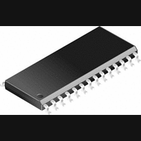
PIC14000-04I/SS Microchip Technology, PIC14000-04I/SS Datasheet - Page 27

PIC14000-04I/SS
Manufacturer Part Number
PIC14000-04I/SS
Description
IC, 8BIT MCU, PIC14, 4MHZ, SSOP-28
Manufacturer
Microchip Technology
Datasheet
1.PIC14000-04SO.pdf
(153 pages)
Specifications of PIC14000-04I/SS
Controller Family/series
PIC14
No. Of I/o's
22
Ram Memory Size
192Byte
Cpu Speed
4MHz
No. Of Timers
2
Interface
I2C
Digital Ic Case Style
SSOP
Core Size
8 Bit
Program Memory Size
4096 X 14
Embedded Interface Type
I2C
Rohs Compliant
Yes
Processor Series
PIC14000
Core
PIC
Data Bus Width
8 bit
Program Memory Type
EPROM
Data Ram Size
192 B
Interface Type
SPI, UART
Maximum Clock Frequency
20 MHz
Number Of Programmable I/os
22
Number Of Timers
1
Operating Supply Voltage
2.7 V to 6 V
Maximum Operating Temperature
+ 85 C
Mounting Style
SMD/SMT
Package / Case
SSOP-28
Development Tools By Supplier
ICE2000
Minimum Operating Temperature
- 40 C
On-chip Adc
14 bit
Lead Free Status / RoHS Status
Lead free / RoHS Compliant
- Current page: 27 of 153
- Download datasheet (767Kb)
This interrupt can wake the device up from SLEEP. The
user, in the interrupt service routine, can clear the
interrupt in one of two ways:
• Disable the interrupt by clearing the RCIE
• Read PORTC. This will end mismatch condition.
A mismatch condition will continue to set the RCIF bit.
Reading PORTC will end the mismatch condition, and
allow the RCIF bit to be cleared.
If bit CMAOE (CMCON<1>) is set, the RC0/REFA pin
becomes the programmable reference A and analog
output. Pin RC1/CMPA becomes the comparator A out-
put.
PORTC<7:6> also serves multiple functions. These
pins act as the I
module is enabled. They also serve as the serial pro-
gramming interface data and clock line for in-circuit
programming of the EPROM.
FIGURE 5-3:
1996 Microchip Technology Inc.
(PIE1<2>) bit
Then, clear the RCIF (PIR1<2>) bit.
Note:
Note:
Setting CMAOE changes the definition of
RC0/REFA and RC1/CMPA, bypassing
the PORTC data and TRISC register set-
tings.
I/O pins have protection diodes to V
2
C data and clock lines when the I
BLOCK DIAGRAM OF PORTC<7:6> PINS
PORTC
TRISC
Write
Write
Data
Bus
Set
RCIF
PORTC
Read
D
CK Q
From other
PORTC pins
D
CK Q
Read
TRISC
Q
Q
I
2
DD
CCON<5>
Preliminary
2
and V
C
SS
. These pins do not have a P-channel pull-up.
The TRISC register controls the direction of the
PORTC pin. A ‘1’ in each location configures the
corresponding port pin as an input. Upon reset, this
register sets to FFh, meaning all PORTC pins are ini-
tially inputs. The data register should be initialized prior
to configuring the port as outputs.
Unused inputs should not be left floating to avoid
leakage currents. All pins have input protection diodes
to V
EXAMPLE 5-2:
CLRF
BSF
MOVLW 0xCF
MOVWF TRISC
Q
Q
DD
EN
EN
Schmitt Trigger
D
D
Input Buffer
and V
PORTC
STATUS, RPO
V
SS
V
SS
DD
N
N
.
Read PORTC
INITIALIZING PORTC
; Initialize PORTC data
;
;
;
; Value used to initialize
; data direction
; Set RC<3:0> as inputs
;
;
; Select Bank1
I/O
Pin
latches before setting
the data direction
register
RC<5:4> as outputs
RC<7:6> as inputs
PIC14000
DS40122B-page 27
Related parts for PIC14000-04I/SS
Image
Part Number
Description
Manufacturer
Datasheet
Request
R

Part Number:
Description:
IC MCU OTP 4KX14 A/D 28SOIC
Manufacturer:
Microchip Technology
Datasheet:

Part Number:
Description:
IC MCU OTP 4KX14 A/D 28SSOP
Manufacturer:
Microchip Technology
Datasheet:

Part Number:
Description:
IC MCU OTP 4KX14 A/D 28SOIC
Manufacturer:
Microchip Technology
Datasheet:

Part Number:
Description:
IC MCU OTP 4KX14 A/D 28DIP
Manufacturer:
Microchip Technology
Datasheet:

Part Number:
Description:
IC MCU OTP 4KX14 A/D 28SSOP
Manufacturer:
Microchip Technology
Datasheet:

Part Number:
Description:
IC MCU OTP 4KX14 A/D 28CDIP
Manufacturer:
Microchip Technology
Datasheet:

Part Number:
Description:
IC MCU OTP 4KX14 A/D 28DIP
Manufacturer:
Microchip Technology
Datasheet:

Part Number:
Description:
IC MCU OTP 4KX14 A/D 28SOIC
Manufacturer:
Microchip Technology
Datasheet:

Part Number:
Description:
IC MCU OTP 4KX14 A/D 28DIP
Manufacturer:
Microchip Technology
Datasheet:

Part Number:
Description:
IC MCU OTP 4KX14 A/D 28DIP
Manufacturer:
Microchip Technology
Datasheet:

Part Number:
Description:
IC MCU OTP 4KX14 A/D 28SOIC
Manufacturer:
Microchip Technology
Datasheet:

Part Number:
Description:
IC MCU OTP 4KX14 A/D 28SSOP
Manufacturer:
Microchip Technology
Datasheet:

Part Number:
Description:
28-Pin Programmable Mixed Signal Controller
Manufacturer:
Microchip Technology
Datasheet:


