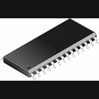
PIC14000-04I/SS Microchip Technology, PIC14000-04I/SS Datasheet - Page 52

PIC14000-04I/SS
Manufacturer Part Number
PIC14000-04I/SS
Description
IC, 8BIT MCU, PIC14, 4MHZ, SSOP-28
Manufacturer
Microchip Technology
Datasheet
1.PIC14000-04SO.pdf
(153 pages)
Specifications of PIC14000-04I/SS
Controller Family/series
PIC14
No. Of I/o's
22
Ram Memory Size
192Byte
Cpu Speed
4MHz
No. Of Timers
2
Interface
I2C
Digital Ic Case Style
SSOP
Core Size
8 Bit
Program Memory Size
4096 X 14
Embedded Interface Type
I2C
Rohs Compliant
Yes
Processor Series
PIC14000
Core
PIC
Data Bus Width
8 bit
Program Memory Type
EPROM
Data Ram Size
192 B
Interface Type
SPI, UART
Maximum Clock Frequency
20 MHz
Number Of Programmable I/os
22
Number Of Timers
1
Operating Supply Voltage
2.7 V to 6 V
Maximum Operating Temperature
+ 85 C
Mounting Style
SMD/SMT
Package / Case
SSOP-28
Development Tools By Supplier
ICE2000
Minimum Operating Temperature
- 40 C
On-chip Adc
14 bit
Lead Free Status / RoHS Status
Lead free / RoHS Compliant
PIC14000
7.5.2
Master mode operation is supported by interrupt
generation on the detection of the START and STOP.
The STOP(P) and START(S) bits are cleared from a
reset or when the I
I
is idle and both the S and P bits are cleared.
In master mode, the SCL and SDA lines are
manipulated
TRISC<7:6> or TRISD<1:0> bits to an output (cleared).
The output level is always low, regardless of the
value(s) in PORTC<7:6> or PORTD<1:0>. So when
transmitting data, a “1” data bit must have the
TRISC<7> or TRISD<1> bit set (input) and a “0” data
bit must have the TRISC<7> or TRISD<1> bit cleared
(output). The same scenario is true for the SCL line
with the TRISC<6> or TRISD<0> bit.
The following events will cause the I
(I
• START
• STOP
• Data transfer byte transmitted/received
Master mode of operation can be done with either the
slave mode idle (I
slave active. When both master and slave modes are
enabled, the software needs to differentiate the
source(s) of the interrupt.
TABLE 7-3:
DS40122B-page 52
2
Address
Legend:
Note: Shaded boxes are not used by the I
2
0B/8Bh
0Ch
8Ch
13h
93h
14h
94h
9Eh
87h
88h
C bus may be taken when the P bit is set, or the bus
CIF) to be set (I
MASTER MODE
r = reserved locations, default is POR value and should not be overwritten with any value
— = Unimplemented location, read as ‘0’
Name
INTCON
PIR1
PIE1
I
I
I
I
MISC
TRISC
TRISD
2
2
2
2
CBUF
CADD
CCON
CSTAT
by
2
REGISTERS ASSOCIATED WITH I
2
2
C interrupt if enabled):
C module is disabled. Control of the
CM3...I
changing
I
I
2
2
SMHOG
TRISC7
TRISD7
C Serial Port Receive Buffer/Transmit Register
C mode Synchronous Serial Port (I
WCOL
CMIF
CMIE
Bit 7
2
GIE
CM0 = 1011b) or with the
—
the
SPGNDB
TRISC6
TRISD6
2
I
C interrupt Flag
2
PEIE
Bit 6
2
CON
C module.
corresponding
—
—
—
SPGNDA
TRISC5
TRISD5
Preliminary
I
2
Bit 5
T0IE
D/A
CEN
—
—
2
C OPERATION
2
C mode) Address Register
TRISC4
TRISD4
I
2
7.5.3
In multi-master mode, the interrupt generation on the
detection of the START and STOP allows the
determination of when the bus is free. The STOP (P)
and START (S) bits are cleared from a reset or when
the I
be taken when the P bit is set, or the bus is idle and
both the S and P bits are cleared. When the bus is
busy, enabling the I
interrupt when the STOP occurs.
In multi-master operation, the SDA line must be
monitored to see if the signal level is the expected
output level. This check only needs to be done when a
high level is output. If a high level is expected and low
level is present, the device needs to release the SDA
and SCL lines (set TRISC<7:6>). There are two stages
where this arbitration can be lost, these are:
• Address Transfer
• Data Transfer
When the slave logic is enabled, the slave continues to
receive. If arbitration was lost during the address
transfer stage, the device may being addressed. If
addressed an ACK pulse will be generated. If
arbitration was lost during the data transfer stage, the
device will need to re-transfer the data at a later time.
PBIE
PBIF
Bit 4
CKP
CSEL
P
r
2
C module is disabled. Control of the I
MULTI-MASTER MODE
SMBUS
TRISC3
TRISD3
I
I
I
2
Bit 3
2
2
CM3
CIF
CIE
S
r
INCLKEN
TRISC2
TRISD2
2
I
C interrupt will generate the
RCIF
RCIE
2
Bit 2
T0IF
R/W
CM2
1996 Microchip Technology Inc.
TRISC1
TRISD1
ADCIF
ADCIE
I
OSC2
2
Bit 1
CM1
UA
r
2
C bus may
TRISC0
TRISD0
OVFIE
OVFIF
I
OSC1
2
Bit 0
CM0
BF
r


