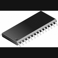
PIC14000-04I/SS Microchip Technology, PIC14000-04I/SS Datasheet - Page 33

PIC14000-04I/SS
Manufacturer Part Number
PIC14000-04I/SS
Description
IC, 8BIT MCU, PIC14, 4MHZ, SSOP-28
Manufacturer
Microchip Technology
Datasheet
1.PIC14000-04SO.pdf
(153 pages)
Specifications of PIC14000-04I/SS
Controller Family/series
PIC14
No. Of I/o's
22
Ram Memory Size
192Byte
Cpu Speed
4MHz
No. Of Timers
2
Interface
I2C
Digital Ic Case Style
SSOP
Core Size
8 Bit
Program Memory Size
4096 X 14
Embedded Interface Type
I2C
Rohs Compliant
Yes
Processor Series
PIC14000
Core
PIC
Data Bus Width
8 bit
Program Memory Type
EPROM
Data Ram Size
192 B
Interface Type
SPI, UART
Maximum Clock Frequency
20 MHz
Number Of Programmable I/os
22
Number Of Timers
1
Operating Supply Voltage
2.7 V to 6 V
Maximum Operating Temperature
+ 85 C
Mounting Style
SMD/SMT
Package / Case
SSOP-28
Development Tools By Supplier
ICE2000
Minimum Operating Temperature
- 40 C
On-chip Adc
14 bit
Lead Free Status / RoHS Status
Lead free / RoHS Compliant
- Current page: 33 of 153
- Download datasheet (767Kb)
FIGURE 5-10: BLOCK DIAGRAM OF PORTD<1:0> PINS
FIGURE 5-11: PORTD DATA REGISTER
Legend: U = unimplemented, read as ‘0’, x = unknown.
08h
PORTD
Read/Write
POR value xxh
B7
B6
B5
B4
B3
B2
B1
B0
1996 Microchip Technology Inc.
Bit
Note: I/O pins have protection diodes to V
RD7/AN7
RD6/AN6
RD5/AN5
RD4/AN4
RD3/REFB
RD2/CMPB
RD1/SDAB
RD0/SCLB
RD7/AN7 RD6/AN6 RD5/AN5 RD4/AN4
Bit 7
R/W
X
Name
PORTD
TRISD
Read
PortD
Write
Write
Bit 6
R/W
Data
Bus
X
GPIO or analog input. Returns value on pin RD7/AN7 when used as a digital
input. When configured as an analog input, reads as ‘0’.
GPIO or analog input. Returns value on pin RD6/AN6 when used as a digital
input. When configured as an analog input, reads as ‘0’.
GPIO or analog input. This pin can connect to a level shift network. If
enabled, a +0.5V offset is added to the input voltage. When configured as
an analog input, reads as ‘0’.
GPIO or analog input. Returns value on pin RD4/AN4 when used as a digital
input. When configured as an analog input, reads as ‘0’.
This pin can serve as a GPIO, or programmable reference B output.
This pin can serve as a GPIO, or comparator B output.
Alternate synchronous serial data I/O for I
the I
purpose I/O. This pin has an N-channel pull-up to VDD which is disabled in
I
Alternate synchronous serial clock for I
I
pose I/O. This pin has an N-Channel pull-up to VDD which is disabled in I
mode.
2
2
C mode.
CSEL bit in the MISC register. This pin can also serve as a general pur-
Bit 5
Function
R/W
D
CK Q
D
CK Q
X
2
CSEL bit in the MISC register. This pin can also serve as a general
TRISD
Read
Q
Q
I
2
Preliminary
CCON<5>
DD
Bit 4
R/W
and V
X
SS
Q
. These pins do not have a P-channel pull-up.
Schmitt Trigger
EN
RD3/REFB
Input Buffer
D
Bit 3
R/W
X
V
SS
V
N
N
DD
RD2/CMPB RD1/SDAB RD0/SCLB
2
C interface, enabled by setting the
Bit 2
R/W
I/O
Pin
X
2
C interface enabled by setting
PIC14000
Bit 1
R/W
X
DS40122B-page 33
Bit 0
R/W
X
2
C
Related parts for PIC14000-04I/SS
Image
Part Number
Description
Manufacturer
Datasheet
Request
R

Part Number:
Description:
IC MCU OTP 4KX14 A/D 28SOIC
Manufacturer:
Microchip Technology
Datasheet:

Part Number:
Description:
IC MCU OTP 4KX14 A/D 28SSOP
Manufacturer:
Microchip Technology
Datasheet:

Part Number:
Description:
IC MCU OTP 4KX14 A/D 28SOIC
Manufacturer:
Microchip Technology
Datasheet:

Part Number:
Description:
IC MCU OTP 4KX14 A/D 28DIP
Manufacturer:
Microchip Technology
Datasheet:

Part Number:
Description:
IC MCU OTP 4KX14 A/D 28SSOP
Manufacturer:
Microchip Technology
Datasheet:

Part Number:
Description:
IC MCU OTP 4KX14 A/D 28CDIP
Manufacturer:
Microchip Technology
Datasheet:

Part Number:
Description:
IC MCU OTP 4KX14 A/D 28DIP
Manufacturer:
Microchip Technology
Datasheet:

Part Number:
Description:
IC MCU OTP 4KX14 A/D 28SOIC
Manufacturer:
Microchip Technology
Datasheet:

Part Number:
Description:
IC MCU OTP 4KX14 A/D 28DIP
Manufacturer:
Microchip Technology
Datasheet:

Part Number:
Description:
IC MCU OTP 4KX14 A/D 28DIP
Manufacturer:
Microchip Technology
Datasheet:

Part Number:
Description:
IC MCU OTP 4KX14 A/D 28SOIC
Manufacturer:
Microchip Technology
Datasheet:

Part Number:
Description:
IC MCU OTP 4KX14 A/D 28SSOP
Manufacturer:
Microchip Technology
Datasheet:

Part Number:
Description:
28-Pin Programmable Mixed Signal Controller
Manufacturer:
Microchip Technology
Datasheet:


