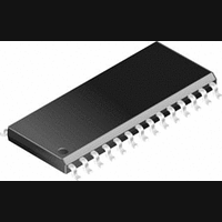
PIC14000-04I/SS Microchip Technology, PIC14000-04I/SS Datasheet - Page 89

PIC14000-04I/SS
Manufacturer Part Number
PIC14000-04I/SS
Description
IC, 8BIT MCU, PIC14, 4MHZ, SSOP-28
Manufacturer
Microchip Technology
Datasheet
1.PIC14000-04SO.pdf
(153 pages)
Specifications of PIC14000-04I/SS
Controller Family/series
PIC14
No. Of I/o's
22
Ram Memory Size
192Byte
Cpu Speed
4MHz
No. Of Timers
2
Interface
I2C
Digital Ic Case Style
SSOP
Core Size
8 Bit
Program Memory Size
4096 X 14
Embedded Interface Type
I2C
Rohs Compliant
Yes
Processor Series
PIC14000
Core
PIC
Data Bus Width
8 bit
Program Memory Type
EPROM
Data Ram Size
192 B
Interface Type
SPI, UART
Maximum Clock Frequency
20 MHz
Number Of Programmable I/os
22
Number Of Timers
1
Operating Supply Voltage
2.7 V to 6 V
Maximum Operating Temperature
+ 85 C
Mounting Style
SMD/SMT
Package / Case
SSOP-28
Development Tools By Supplier
ICE2000
Minimum Operating Temperature
- 40 C
On-chip Adc
14 bit
Lead Free Status / RoHS Status
Lead free / RoHS Compliant
FIGURE 10-13: WAKE-UP FROM SLEEP AND HIBERNATE THROUGH INTERRUPT
10.9
The code in the program memory can be protected by
programming the code protect bits. When code
protected, the contents of the program memory cannot
be read out. In code-protected mode, the configuration
word (2007h) will not be scrambled, allowing reading of
all configuration bits.
10.10
PIC14000 can be serially programmed while in the end
application circuit. This is simply done with two lines for
clock and data, and three other lines for power, ground
and the programming voltage. This allows customers to
manufacture boards with unprogrammed devices, and
then program the microcontroller just before shipping
the product. This allows the most recent firmware or a
custom firmware to be programmed.
The device is placed into a program/verify mode by
holding the RC6/SCL and RC7/SDA pins low while
raising the MCLR (V
becomes the programming clock and RC7 becomes
the programmed data. Both RC6 and RC7 are Schmitt
trigger inputs in this mode.
1996 Microchip Technology Inc.
INSTRUCTION FLOW
INTERRUPT
Flag (5)
GIE bit
(INTCON<7>)
Note 1:
Instruction
fetched
CLKOUT(4)
Instruction
executed
Code Protection
In-Circuit Serial Programming
OSC1
2:
3:
4:
5:
PC
HS oscillator mode assumed.
T
GIE = 1 assumed. In this case after wake up processor jumps to interrupt routine. If GIE = 0, execution will continue in line.
CLKOUT is not available in these osc modes, but shown here for timing reference.
Refer to Section 10.8 for sources.
Inst(PC) = SLEEP
Q1 Q2 Q3 Q4 Q1 Q2 Q3 Q4 Q1
OST
Inst(PC - 1)
= 1024 T
PP
PC
) pin from V
OSC
(drawing not to scale). This delay will be 8 T
Inst(PC + 1)
SLEEP
PC+1
IL
to V
IH
Processor in
. RC6 then
SLEEP
PC+2
Preliminary
T
OST
(2)
Q1 Q2 Q3 Q4 Q1 Q2 Q3 Q4 Q1 Q2 Q3 Q4 Q1 Q2 Q3 Q4
Inst(PC + 2)
Inst(PC + 1)
After reset, to place the device into programming/verify
mode, the program counter (PC) is at location 00h. A
6-bit command is then supplied to the device.
Depending on the command, 14-bits of program data
are then supplied to or from the device. For complete
details about serial programming, please refer to the
PIC16C6X/7X Programming Specifications (Literature
#DS30228).
A typical in-system serial programming connection is
shown in Figure 10-14.
FIGURE 10-14: TYPICAL IN-SYSTEM SERIAL
OSC
External
Connector
Signals
Data I/O
for IN osc mode.
CLK
+5V
Vpp
Interrupt Latency
Dummy cycle
0V
(Note 2)
PC + 2
PROGRAMMING
CONNECTION
To Normal
Connections
To Normal
Connections
Inst(0004h)
Dummy cycle
0004h
PIC14000
Inst(0005h)
DS40122B-page 89
Inst(0004h)
V
V
MCLR/V
RC6
RC7
0005h
DD
SS
PIC14000
V
PP
DD


