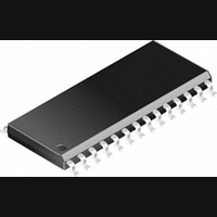
PIC14000-04I/SS Microchip Technology, PIC14000-04I/SS Datasheet - Page 45

PIC14000-04I/SS
Manufacturer Part Number
PIC14000-04I/SS
Description
IC, 8BIT MCU, PIC14, 4MHZ, SSOP-28
Manufacturer
Microchip Technology
Datasheet
1.PIC14000-04SO.pdf
(153 pages)
Specifications of PIC14000-04I/SS
Controller Family/series
PIC14
No. Of I/o's
22
Ram Memory Size
192Byte
Cpu Speed
4MHz
No. Of Timers
2
Interface
I2C
Digital Ic Case Style
SSOP
Core Size
8 Bit
Program Memory Size
4096 X 14
Embedded Interface Type
I2C
Rohs Compliant
Yes
Processor Series
PIC14000
Core
PIC
Data Bus Width
8 bit
Program Memory Type
EPROM
Data Ram Size
192 B
Interface Type
SPI, UART
Maximum Clock Frequency
20 MHz
Number Of Programmable I/os
22
Number Of Timers
1
Operating Supply Voltage
2.7 V to 6 V
Maximum Operating Temperature
+ 85 C
Mounting Style
SMD/SMT
Package / Case
SSOP-28
Development Tools By Supplier
ICE2000
Minimum Operating Temperature
- 40 C
On-chip Adc
14 bit
Lead Free Status / RoHS Status
Lead free / RoHS Compliant
- Current page: 45 of 153
- Download datasheet (767Kb)
7.3
All data must be transmitted per byte, with no limit to
the number of bytes transmitted per data transfer. After
each
acknowledge bit (ACK). This is shown in Figure 7-6.
When a slave-receiver doesn’t acknowledge the slave
address or received data, the master must abort the
transfer. The slave must leave SDA high so that the
master can generate the STOP (Figure 7-1).
If the master is receiving the data (master-receiver), it
generates an acknowledge signal for each received
byte of data, except for the last byte. To signal the end
of data to the slave-transmitter, the master does not
generate an acknowledge. The slave then releases the
SDA line so the master can generate the STOP. The
master can also generate the STOP during the
acknowledge pulse for valid termination of data
transfer.
If the slave needs to delay the transmission of the next
byte, holding the SCL line low will force the master into
a wait state. Data transfer continues when the slave
releases the SCL line. This allows the slave to move
the received data or fetch the data it needs to transfer
before allowing the clock to start. This wait state can be
FIGURE 7-7:
1996 Microchip Technology Inc.
SDA
SCL
byte,
Transfer Acknowledge
Condition
Start
S
the
SAMPLE I
MSB
slave-receiver
1
Address
2
2
C DATA TRANSFER
acknowledgement
signal from receiver
generates
7
R/W
8
Preliminary
an
ACK
9
byte complete.
interrupt with receiver
Wait
State
accomplished by setting SMHOG (MISC<7>) high.
Clearing MISC<7> will resume the data transfer.
Figure 7-7 shows a data transfer waveform.
Figure 7-8 and Figure 7-9 show master-transmitter and
master-receiver data transfer sequences.
FIGURE 7-6:
clock line held low while
interrupts are serviced
1
Transmitter
Output by
Output by
SCL from
Receiver
Master
Data
Data
Data
2
Condition
Start
S
acknowledgement
signal from receiver
3 • 8
I
ACKNOWLEDGE
2
C SLAVE-RECEIVER
1
ACK
9
2
PIC14000
not acknowledge
Condition
acknowledge
DS40122B-page 45
Stop
8
P
acknowledgement
Clock pulse for
9
Related parts for PIC14000-04I/SS
Image
Part Number
Description
Manufacturer
Datasheet
Request
R

Part Number:
Description:
IC MCU OTP 4KX14 A/D 28SOIC
Manufacturer:
Microchip Technology
Datasheet:

Part Number:
Description:
IC MCU OTP 4KX14 A/D 28SSOP
Manufacturer:
Microchip Technology
Datasheet:

Part Number:
Description:
IC MCU OTP 4KX14 A/D 28SOIC
Manufacturer:
Microchip Technology
Datasheet:

Part Number:
Description:
IC MCU OTP 4KX14 A/D 28DIP
Manufacturer:
Microchip Technology
Datasheet:

Part Number:
Description:
IC MCU OTP 4KX14 A/D 28SSOP
Manufacturer:
Microchip Technology
Datasheet:

Part Number:
Description:
IC MCU OTP 4KX14 A/D 28CDIP
Manufacturer:
Microchip Technology
Datasheet:

Part Number:
Description:
IC MCU OTP 4KX14 A/D 28DIP
Manufacturer:
Microchip Technology
Datasheet:

Part Number:
Description:
IC MCU OTP 4KX14 A/D 28SOIC
Manufacturer:
Microchip Technology
Datasheet:

Part Number:
Description:
IC MCU OTP 4KX14 A/D 28DIP
Manufacturer:
Microchip Technology
Datasheet:

Part Number:
Description:
IC MCU OTP 4KX14 A/D 28DIP
Manufacturer:
Microchip Technology
Datasheet:

Part Number:
Description:
IC MCU OTP 4KX14 A/D 28SOIC
Manufacturer:
Microchip Technology
Datasheet:

Part Number:
Description:
IC MCU OTP 4KX14 A/D 28SSOP
Manufacturer:
Microchip Technology
Datasheet:

Part Number:
Description:
28-Pin Programmable Mixed Signal Controller
Manufacturer:
Microchip Technology
Datasheet:


