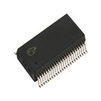
CY7C63413-PVXC Cypress Semiconductor Corp, CY7C63413-PVXC Datasheet - Page 13

CY7C63413-PVXC
Manufacturer Part Number
CY7C63413-PVXC
Description
Manufacturer
Cypress Semiconductor Corp
Datasheet
1.CY7C63413-PVXC.pdf
(32 pages)
Specifications of CY7C63413-PVXC
Cpu Family
enCoRe II
Device Core
M8C
Device Core Size
8b
Frequency (max)
12MHz
Interface Type
USB
Program Memory Type
EPROM
Program Memory Size
8KB
Total Internal Ram Size
256Byte
# I/os (max)
24
Number Of Timers - General Purpose
1
Operating Supply Voltage (typ)
5V
Operating Supply Voltage (max)
5.25/5.5V
Operating Supply Voltage (min)
4/4.35V
Instruction Set Architecture
RISC
Operating Temp Range
0C to 70C
Operating Temperature Classification
Commercial
Mounting
Surface Mount
Pin Count
48
Package Type
SSOP
Lead Free Status / Rohs Status
Compliant
Document #: 38-08027 Rev. *B
Table 11.Possible Port Configurations
In “Resistive” mode, a 7-kΩ pull-up resistor is conditionally
enabled for all pins of a GPIO port. The resistor is enabled for
any pin that has been written as a “1.” The resistor is disabled
on any pin that has been written as a “0.” An I/O pin will be
driven high through a 7-kΩ pull-up resistor when a “1” has
been written to the pin. Or the output pin will be driven LOW,
with the pull-up disabled, when a “0” has been written to the
pin. An I/O pin that has been written as a “1” can be used as
an input pin with an integrated 7-kΩ pull-up resistor. Resistive
mode selects a negative (falling edge) interrupt polarity on all
pins that have the GPIO interrupt enabled.
In “CMOS” mode, all pins of the GPIO port are outputs that are
actively driven. The current source and sink capacity are
roughly the same (symmetric output drive). A CMOS port is not
a possible source for interrupts.
A port configured in CMOS mode has interrupt generation
disabled, yet the interrupt mask bits serve to control port
DAC Port
Config Bit 1
Port Configuration bits
Port 3
W
7
Addr: 0x08
11
10
10
01
00
Internal
Data Bus
Config Bit 0
Port 3
W
6
Interrupt
Enable
Interrupt
Polarity
Config Bit 1
Internal
Buffer
Port 2
DAC Write
DAC Read
W
Pin Interrupt Bit
Data
Out
Latch
5
Table 12.GPIO Configuration Register
Figure 5. Block Diagram of DAC Port
X
X
X
0
1
GPIO Configuration Register
Config Bit 0
Isink
Register
Port 2
W
4
4 bits
Isink
DAC
direction. If a port’s associated Interrupt Mask bits are cleared,
those port bits are strictly outputs. If the Interrupt Mask bits are
set then those bits will be open drain inputs. As open drain
inputs, if their data output values are ‘1’ those port pins will be
CMOS inputs (HIGH Z output).
In “Open Drain” mode the internal pull-up resistor and CMOS
driver (HIGH) are both disabled. An I/O pin that has been
written as a “1” can be used as either a high-impedance input
or a three-state output. An I/O pin that has been written as a
“0” will drive the output LOW. The interrupt polarity for an open
drain GPIO port can be selected as either positive (rising
edge) or negative (falling edge).
During reset, all of the bits in the GPIO Configuration Register
are written with “0.” This selects the default configuration:
Open Drain output, positive interrupt polarity for all GPIO
ports.
Config Bit 1
to Interrupt
Controller
Port 1
W
3
CMOS Output
Driver Mode
V
Open Drain
Open Drain
Open Drain
CC
Resistive
Q1
14 KΩ
Config Bit 0
Port 1
W
2
ESD
DAC
I/O Pin
Config Bit 1
Port 0
Interrupt Polarity
W
1
CY7C63413C
CY7C63513C
CY7C63613C
+ (default)
disabled
disabled
-
-
Page 13 of 32
Config Bit 0
Port 0
W
0
[+] Feedback


