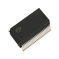
CY7C63413-PVXC Cypress Semiconductor Corp, CY7C63413-PVXC Datasheet - Page 25

CY7C63413-PVXC
Manufacturer Part Number
CY7C63413-PVXC
Description
Manufacturer
Cypress Semiconductor Corp
Datasheet
1.CY7C63413-PVXC.pdf
(32 pages)
Specifications of CY7C63413-PVXC
Cpu Family
enCoRe II
Device Core
M8C
Device Core Size
8b
Frequency (max)
12MHz
Interface Type
USB
Program Memory Type
EPROM
Program Memory Size
8KB
Total Internal Ram Size
256Byte
# I/os (max)
24
Number Of Timers - General Purpose
1
Operating Supply Voltage (typ)
5V
Operating Supply Voltage (max)
5.25/5.5V
Operating Supply Voltage (min)
4/4.35V
Instruction Set Architecture
RISC
Operating Temp Range
0C to 70C
Operating Temperature Classification
Commercial
Mounting
Surface Mount
Pin Count
48
Package Type
SSOP
Lead Free Status / Rohs Status
Compliant
Document #: 38-08027 Rev. *B
Absolute Maximum Ratings
Storage Temperature ..........................................................................................................................................–65°C to +150°C
Ambient Temperature with Power Applied ...............................................................................................................–0°C to +70°C
Supply Voltage on V
DC Input Voltage........................................................................................................................................... –0.5V to +V
DC Voltage Applied to Outputs in High Z State............................................................................................ –0.5V to + V
Max. Output Current into Port 0,1,2,3 and DAC[1:0] Pins ................................................................................................... 60 mA
Max. Output Current into DAC[7:2] Pins ............................................................................................................................. 10 mA
Power Dissipation ............................................................................................................................................................. 300 mW
Static Discharge Voltage ............................................................................................................................................... > 2000V
Latch-up Current ........................................................................................................................................................... > 200 mA
DC Characteristics
V
V
I
I
I
V
T
t
t
t
I
I
t
V
V
V
V
V
C
I
R
R
R
R
V
Notes:
CC1
CC2
SB1
int1
int2
watch
il
sm
vccs
lo
3. Qualified with JEDEC EIA/JESD22-A114-B test method.
4. Functionality is guaranteed of the V
5. USB transmitter functionality is guaranteed over the V
6. Total current cumulative across all Port pins flowing to V
7. Port 3 bit 7 controls whether the parts goes into suspend after a POR event or waits 128 ms to begin running.
8. POR will re-occur whenever V
General
Power-On Reset
USB Interface
General Purpose I/O Interface
start
CC (1)
CC (2)
PP
oh
ol
di
cm
se
pu
pu
pd
ith
in
up
Operating Voltage
Operating Voltage
V
V
Supply Current - Suspend Mode
Programming Voltage (disabled)
Resonator Start-up Interval
Internal Timer #1 Interrupt Period
Internal Timer #2 Interrupt Period
Watch Dog Timer Period
Input Leakage Current
Max I
V
Static Output HIGH
Static Output LOW
Differential Input Sensitivity
Differential Input Common Mode Range
Single-Ended Receiver Threshold
Transceiver Capacitance
Hi-Z State Data Line Leakage
Bus Pull-up Resistance (V
Bus Pull-up Resistance (Ext. 3.3V option)
Bus Pull-down Resistance
Pull-up Resistance
Input Threshold Voltage
CC
CC
CC
Operating Supply Current
= 4.35V
Reset Slew
SS
CC
IO Sink Current
relative to V
Fosc = 6 MHz; Operating Temperature = 0 to 70°C
CC
drops to approximately 2.5V.
Parameter
CC (1)
SS
range, except USB transmitter and DACs.
.................................................................................................................... –0.5V to +7.0V
CC
option)
CC (2)
SS
is limited to minimize Ground-Drop noise effects.
range, as well as DAC outputs.
7.35K
1.024
8.192
0.001
1.425
14.25
4.9K
Min.
4.35
–0.4
45%
128
–10
4.0
2.8
0.2
0.8
0.8
1.024
14.33
1.575
15.75
Max.
9.1K
5.25
7.65
65%
256
128
200
5.5
0.4
3.6
0.3
2.5
2.0
40
15
30
60
20
10
1
Ohms
Unit
V
mA
mA
mA
ms
ms
ms
kΩ
µA
µA
pF
µA
µs
µs
kΩ
kΩ
V
V
V
V
V
V
V
V
CC
Non USB activity (note 4)
USB activity (note 5)
V
Oscillator off, D– > Voh min
V
Any pin
Cumulative across all ports (note 6)
Linear ramp: 0 to 4.35V (notes 7,8)
15k ± 5% ohms to Gnd (note 5)
|(D+)–(D–)|
9-1
0 V < V
7.5 kΩ ± 2% to V
1.5 kΩ ± 5% to 3.0–3.6V
15 kΩ ± 5%
All ports, LOW to HIGH edge
CC
CC
= 5.5V
= 5.0V, ceramic resonator
in
<3.3 V
Conditions
CY7C63413C
CY7C63513C
CY7C63613C
CC
Page 25 of 32
CC
CC
+0.5V
+0.5V
[3]
[+] Feedback


