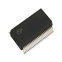
CY7C63413-PVXC Cypress Semiconductor Corp, CY7C63413-PVXC Datasheet - Page 15

CY7C63413-PVXC
Manufacturer Part Number
CY7C63413-PVXC
Description
Manufacturer
Cypress Semiconductor Corp
Datasheet
1.CY7C63413-PVXC.pdf
(32 pages)
Specifications of CY7C63413-PVXC
Cpu Family
enCoRe II
Device Core
M8C
Device Core Size
8b
Frequency (max)
12MHz
Interface Type
USB
Program Memory Type
EPROM
Program Memory Size
8KB
Total Internal Ram Size
256Byte
# I/os (max)
24
Number Of Timers - General Purpose
1
Operating Supply Voltage (typ)
5V
Operating Supply Voltage (max)
5.25/5.5V
Operating Supply Voltage (min)
4/4.35V
Instruction Set Architecture
RISC
Operating Temp Range
0C to 70C
Operating Temperature Classification
Commercial
Mounting
Surface Mount
Pin Count
48
Package Type
SSOP
Lead Free Status / Rohs Status
Compliant
Document #: 38-08027 Rev. *B
USB Serial Interface Engine (SIE)
The SIE allows the microcontroller to communicate with the
USB host. The SIE simplifies the interface between the micro-
controller and USB by incorporating hardware that handles the
following USB bus activity independently of the microcon-
troller:
Firmware is required to handle the rest of the USB interface
with the following tasks:
USB Enumeration
The enumeration sequence is shown below:
Table 17.USB Status and Control Register
1. The host computer sends a Setup packet followed by a
2. The USB Controller decodes the request and retrieves its
3. The host computer performs a control read sequence and
4. After receiving the descriptor, the host computer sends a
5. The USB Controller stores the new address in its USB
6. The host sends a request for the Device descriptor using
• Bit stuffing/unstuffing
• Checksum generation/checking
• ACK/NAK
• Token type identification
• Address checking
• Coordinate enumeration by responding to set-up packets
• Fill and empty the FIFOs
• Suspend/Resume coordination
• Verify and select Data toggle values
Data packet to USB address 0 requesting the Device de-
scriptor.
Device descriptor from the program memory space.
the USB Controller responds by sending the Device
descriptor over the USB bus.
Setup packet followed by a Data packet to address 0
assigning a new USB address to the device.
Device Address Register after the no-data control
sequence is complete.
the new USB address.
Reserved
7
Addr:0x1F
Reserved
6
D+
R
5
USB Status and Control Register
D–
R
4
10.The USB Controller retrieves the descriptors from its
PS/2 Operation
PS/2 operation is possible with the CY7C63413C/513C/613C
series through the use of firmware and several operating
modes. The first enabling feature:
Bits 5 and 4 of the Upstream Status and Control register are
directly connected to the D+ and D− USB pins of the
CY7C63413C/513C/613C. These pins constantly monitor the
levels of these signals with CMOS input thresholds. Firmware
can poll and decode these signals as PS/2 clock and data.
Bits [2:0] defaults to ‘000’ at reset which allows the USB SIE
to control output on D+ and D−. Firmware can override the SIE
and directly control the state of these pins via these 3 control
bits. Since PS/2 is an open drain signaling protocol, these
modes allow all 4 PS/2 states to be generated on the D+ and
D− pins
USB Port Status and Control
USB status and control is regulated by the USB Status and
Control Register located at I/O address 0x1F as shown in
Figure 17. This is a read/write register. All reserved bits must
be written to zero. All bits in the register are cleared during
reset.
Bus Activity
7. The USB Controller decodes the request and retrieves the
8. The host performs a control read sequence and the USB
9. The host generates control reads to the USB Controller to
1. USB Bus reset on D+ and D− is an interrupt that can be
2. USB traffic can be disabled via bit 7 of the USB register;
3. D+ and D− can be monitored and driven via firmware as
Device descriptor from the program memory.
Controller responds by sending its Device descriptor over
the USB bus.
request the Configuration and Report descriptors.
program space and returns the data to the host over the
USB.
disabled;
independent port bits.
R/W
3
Control
Bit 2
R/W
2
Control
Bit 1
R/W
1
CY7C63413C
CY7C63513C
CY7C63613C
Page 15 of 32
Control
Bit 0
R/W
0
[+] Feedback


