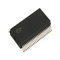
CY7C63413-PVXC Cypress Semiconductor Corp, CY7C63413-PVXC Datasheet - Page 18

CY7C63413-PVXC
Manufacturer Part Number
CY7C63413-PVXC
Description
Manufacturer
Cypress Semiconductor Corp
Datasheet
1.CY7C63413-PVXC.pdf
(32 pages)
Specifications of CY7C63413-PVXC
Cpu Family
enCoRe II
Device Core
M8C
Device Core Size
8b
Frequency (max)
12MHz
Interface Type
USB
Program Memory Type
EPROM
Program Memory Size
8KB
Total Internal Ram Size
256Byte
# I/os (max)
24
Number Of Timers - General Purpose
1
Operating Supply Voltage (typ)
5V
Operating Supply Voltage (max)
5.25/5.5V
Operating Supply Voltage (min)
4/4.35V
Instruction Set Architecture
RISC
Operating Temp Range
0C to 70C
Operating Temperature Classification
Commercial
Mounting
Surface Mount
Pin Count
48
Package Type
SSOP
Lead Free Status / Rohs Status
Compliant
Document #: 38-08027 Rev. *B
12-bit Free-running Timer
The 12-bit timer provides two interrupts (128 µs and 1.024 ms)
and allows the firmware to directly time events that are up to
4 ms in duration. The lower 8 bits of the timer can be read
directly by the firmware. Reading the lower 8 bits latches the
Timer (LSB)
Table 22.Timer Register
Timer (MSB)
Table 23.Timer Register
Processor Status and Control Register
Table 24.Processor Status and Control Register
The “Run” (bit 0) is manipulated by the HALT instruction. When
Halt is executed, the processor clears the run bit and halts at
the end of the current instruction. The processor remains
Reserved
Pending
Timer
Bit 7
IRQ
R
R
7
Addr: 0xFF
Addr: 0x24
Addr: 0x25
11
L3
D3
Watch Dog
Reserved
10
Timer
L2
Reset
Bit 6
R/W
R
D2
6
9
L1
D1
8
L0
Reserved
USB Bus
D0
Timer
Reset
Bit 5
R/W
R
5
7
D7
Processor Status and Control Register
6
Figure 6. Timer Block Diagram
D6
Reserved
Power-on
Timer Register (MSB)
Timer Register (LSB)
5
Timer
Reset
Bit 4
R/W
D5
R
4
4
D4
Suspend, Wait
3
upper 4 bits into a temporary register. When the firmware
reads the upper 4 bits of the timer, it is actually reading the
count stored in the temporary register. The effect of this logic
is to ensure a stable 12-bit timer value can be read, even when
the two reads are separated in time.
halted until a reset (Power On or Watch Dog). Notice, when
writing to the processor status and control register, the run bit
should always be written as a “1.”
for Interrupt
D3
Timer
Timer
Bit 11
Bit 3
R/W
R
R
2
3
D2
1
D1
8
Interrupt
0
Timer
Timer
Bit 10
Mask
Bit 2
D0
R
R
R
2
1.024-ms interrupt
128-
1-MHz clock
To Timer Register
Single Step
µ
Timer
Timer
POR Default: 0x0101
Bit 1
Bit 9
s interrupt
R/W
R
R
WDC Reset: 0x41
1
CY7C63413C
CY7C63513C
CY7C63613C
Page 18 of 32
Timer
Timer
Bit 0
Bit 8
R/W
Run
R
R
0
[+] Feedback


