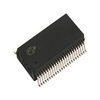
CY7C63413-PVXC Cypress Semiconductor Corp, CY7C63413-PVXC Datasheet - Page 17

CY7C63413-PVXC
Manufacturer Part Number
CY7C63413-PVXC
Description
Manufacturer
Cypress Semiconductor Corp
Datasheet
1.CY7C63413-PVXC.pdf
(32 pages)
Specifications of CY7C63413-PVXC
Cpu Family
enCoRe II
Device Core
M8C
Device Core Size
8b
Frequency (max)
12MHz
Interface Type
USB
Program Memory Type
EPROM
Program Memory Size
8KB
Total Internal Ram Size
256Byte
# I/os (max)
24
Number Of Timers - General Purpose
1
Operating Supply Voltage (typ)
5V
Operating Supply Voltage (max)
5.25/5.5V
Operating Supply Voltage (min)
4/4.35V
Instruction Set Architecture
RISC
Operating Temp Range
0C to 70C
Operating Temperature Classification
Commercial
Mounting
Surface Mount
Pin Count
48
Package Type
SSOP
Lead Free Status / Rohs Status
Compliant
Document #: 38-08027 Rev. *B
The ‘Acknowledge’ bit is set whenever the SIE engages in a
transaction that completes with an ‘ACK’ packet.
The ‘set-up’ PID status (bit[7]) is forced HIGH from the start of
the data packet phase of the set-up transaction, until the start
of the ACK packet returned by the SIE. The CPU is prevented
from clearing this bit during this interval, and subsequently
until the CPU first does an IORD to this endpoint 0 mode
register.
Bits[6:0] of the endpoint 0 mode register are locked from CPU
IOWR operations only if the SIE has updated one of these bits,
which the SIE does only at the end of a packet transaction (set-
up... Data... ACK, or Out... Data... ACK, or In... Data... ACK).
The CPU can unlock these bits by doing a subsequent I/O read
of this register.
Firmware must do an IORD after an IOWR to an endpoint 0
register to verify that the contents have changed and that the
SIE has not updated these values.
Table 21.USB Device Counter Registers
Data 0/1
Addr: 0x11, 0x13, 0x15
Toggle
R/W
Data Valid
R/W
Reserved
R/W
USB Device Counter Registers
Reserved
R/W
While the ‘set-up’ bit is set, the CPU cannot write to the DMA
buffers at memory locations 0xE0 through 0xE7 and 0xF8
through 0xFF. This prevents an incoming set-up transaction
from conflicting with a previous In data buffer filling operation
by firmware.
The mode bits (bits [3:0]) in an Endpoint Mode Register control
how the endpoint responds to USB bus traffic. The mode bit
encoding is shown in Section .
The format of the endpoint Device counter registers is shown
in Table 21.
Bits 0 to 3 indicate the number of data bytes to be transmitted
during an IN packet, valid values are 0 to 8 inclusive. Data
Valid bit 6 is used for OUT and set-up tokens only. Data 0/1
Toggle bit 7 selects the DATA packet’s toggle state: 0 for
DATA0, 1 for DATA1.
Byte count
Bit 3
R/W
Byte count
Bit 2
R/W
Byte count
Bit 1
R/W
CY7C63413C
CY7C63513C
CY7C63613C
Page 17 of 32
Byte count
Bit 0
R/W
[+] Feedback


