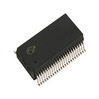
CY7C63413-PVXC Cypress Semiconductor Corp, CY7C63413-PVXC Datasheet - Page 4

CY7C63413-PVXC
Manufacturer Part Number
CY7C63413-PVXC
Description
Manufacturer
Cypress Semiconductor Corp
Datasheet
1.CY7C63413-PVXC.pdf
(32 pages)
Specifications of CY7C63413-PVXC
Cpu Family
enCoRe II
Device Core
M8C
Device Core Size
8b
Frequency (max)
12MHz
Interface Type
USB
Program Memory Type
EPROM
Program Memory Size
8KB
Total Internal Ram Size
256Byte
# I/os (max)
24
Number Of Timers - General Purpose
1
Operating Supply Voltage (typ)
5V
Operating Supply Voltage (max)
5.25/5.5V
Operating Supply Voltage (min)
4/4.35V
Instruction Set Architecture
RISC
Operating Temp Range
0C to 70C
Operating Temperature Classification
Commercial
Mounting
Surface Mount
Pin Count
48
Package Type
SSOP
Lead Free Status / Rohs Status
Compliant
Document #: 38-08027 Rev. *B
Pin Definitions
Programming Model
14-bit Program Counter (PC)
The 14-bit Program Counter (PC) allows access for up to 8
kilobytes of EPROM using the CY7C63413C/513C/613C
architecture. The program counter is cleared during reset,
such that the first instruction executed after a reset is at
address 0x0000. This is typically a jump instruction to a reset
handler that initializes the application.
The lower eight bits of the program counter are incremented
as instructions are loaded and executed. The upper six bits of
the program counter are incremented by executing an XPAGE
instruction. As a result, the last instruction executed within a
256-byte “page” of sequential code should be an XPAGE
instruction. The assembler directive “XPAGEON” will cause
the assembler to insert XPAGE instructions automatically. As
instructions can be either one or two bytes long, the assembler
may occasionally need to insert a NOP followed by an XPAGE
for correct execution.
The program counter of the next instruction to be executed,
carry flag, and zero flag are saved as two bytes on the program
stack during an interrupt acknowledge or a CALL instruction.
The program counter, carry flag, and zero flag are restored
from the program stack only during a RETI instruction.
D+, D–
P0[7:0]
P1[3:0]
P2
P3[7:4]
DAC
XTAL
XTAL
V
V
Vss
Name
PP
CC
IN
OUT
OUT
I/O
I/O
I/O
I/O
I/O
I/O
I/O
IN
11,30,12,
29,13,28,
15,26,16
25,17,24
33,9,32,
37,5,36,
40-Pin
7,34,8,
3,38,4,
18,23
14,27
10,31
20,39
6,35
1,2
n/a
21
22
19
40
CY7C63413C
11,38,12,
37,13,36,
17,32,18
31,19,30
41,9,40,
45,5,44,
48-Pin
7,42,8,
3,46,4,
20,29
14,35
10,39
24,47
6,43
1,2
n/a
25
26
23
48
17,32,18,
31,19,30,
37,13,36,
15,34,16,
33,21,28,
11,38,12,
41,9,40,
45,5,44,
7,42,8,
3,46,4,
20,29
14,35
10,39
22,27
24,47
6,43
Die
1,2
25
26
23
48
CY7C63513C CY7C63613C
17,32,18,31,
15,34,16,33,
11,38,12,37,
19,30,20,29
13,36,14,35
7,42,8,41,9,
3,46,4,45,5,
21,28,22,27
40,10,39
44,6,43
48-Pin
24,47
1,2
25
26
23
48
Please note the program counter cannot be accessed directly
by the firmware. The program stack can be examined by
reading SRAM from location 0x00 and up.
8-bit Accumulator (A)
The accumulator is the general purpose, do everything
register in the architecture where results are usually calcu-
lated.
8-bit Index Register (X)
The index register “X” is available to the firmware as an
auxiliary accumulator. The X register also allows the processor
to perform indexed operations by loading an index value into
X.
8-bit Program Stack Pointer (PSP)
During a reset, the Program Stack Pointer (PSP) is set to zero.
This means the program “stack” starts at RAM address 0x00
and “grows” upward from there. Note the program stack
pointer is directly addressable under firmware control, using
the MOV PSP,A instruction. The PSP supports interrupt
service under hardware control and CALL, RET, and RETI
instructions under firmware control.
7, 18, 8, 17, 9,
5, 20, 6, 19
3, 22, 4, 21
16, 10, 15
24-Pin
12, 23
1,2
n/a
n/a
13
14
11
24
USB differential data; PS/2 clock and
data signals
GPIO port 0 capable of sinking 7 mA
(typical)
GPIO Port 1 capable of sinking 7 mA
(typical).
GPIO Port 2 capable of sinking 7 mA
(typical).
GPIO Port 3 capable of sinking 12 mA
(typical).
DAC I/O Port with programmable
current sink outputs. DAC[1:0] offer a
programmable range of 3.2 to 16 mA
typical. DAC[7:2] have a program-
mable sink current range of 0.2 to 1.0
mA typical. DAC I/O Port not bonded
out on CY7C63613C. See note on
page 12 for firmware code needed for
unused pins.
6-MHz ceramic resonator or external
clock input
6-MHz ceramic resonator
Programming voltage supply, ground
during operation
Voltage supply
Ground
Description
CY7C63413C
CY7C63513C
CY7C63613C
Page 4 of 32
[+] Feedback


