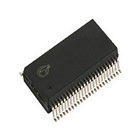
CY7C63413-PVXC Cypress Semiconductor Corp, CY7C63413-PVXC Datasheet - Page 14

CY7C63413-PVXC
Manufacturer Part Number
CY7C63413-PVXC
Description
Manufacturer
Cypress Semiconductor Corp
Datasheet
1.CY7C63413-PVXC.pdf
(32 pages)
Specifications of CY7C63413-PVXC
Cpu Family
enCoRe II
Device Core
M8C
Device Core Size
8b
Frequency (max)
12MHz
Interface Type
USB
Program Memory Type
EPROM
Program Memory Size
8KB
Total Internal Ram Size
256Byte
# I/os (max)
24
Number Of Timers - General Purpose
1
Operating Supply Voltage (typ)
5V
Operating Supply Voltage (max)
5.25/5.5V
Operating Supply Voltage (min)
4/4.35V
Instruction Set Architecture
RISC
Operating Temp Range
0C to 70C
Operating Temperature Classification
Commercial
Mounting
Surface Mount
Pin Count
48
Package Type
SSOP
Lead Free Status / Rohs Status
Compliant
Document #: 38-08027 Rev. *B
Table 13.DAC Port Data
The DAC port provides the CY7C63513C with 8 program-
mable current sink I/O pins. Writing a “1” to a DAC I/O pin
disables the output current sink (Isink DAC) and drives the I/O
pin HIGH through an integrated 14 Kohm resistor. When a “0”
is written to a DAC I/O pin, the Isink DAC is enabled and the
pull-up resistor is disabled. A “0” output will cause the Isink
DAC to sink current to drive the output LOW. The amount of
sink current for the DAC I/O pin is programmable over 16
values based on the contents of the DAC Isink Register for that
output pin. DAC[1:0] are the two high current outputs that are
programmable from a minimum of 3.2 mA to a maximum of 16
mA (typical). DAC[7:2] are low current outputs that are
programmable from a minimum of 0.2 mA to a maximum of 1.0
mA (typical).
When a DAC I/O bit is written as a “1,” the I/O pin is either an
output pulled high through the 14 Kohm resistor or an input
with an internal 14 Kohm pull-up resistor. All DAC port data bits
are set to “1” during reset.
DAC Port Interrupts
A DAC port interrupt can be enabled/disabled for each pin
individually. The DAC Port Interrupt Enable register provides
Table 14.DAC Port Interrupt Enable
Table 15.DAC Port Interrupt Polarity
Table 16.DAC Port Isink
DAC[7]
DAC[7]
DAC[7]
R/W
W
W
Addr: 0x38-0x3F
Addr: 0x30
Addr: 0x31
Addr: 0x32
DAC[6]
DAC[6]
DAC[6]
R/W
W
W
Reserved
0.2 mA to 1.0 mA typical
DAC[5]
DAC[5]
DAC[5]
R/W
Low current outputs
W
W
DAC Port Interrupt Polarity
DAC Port Interrupt Polarity
DAC Port Interrupt Enable
DAC[4]
DAC[4]
DAC[4]
R/W
W
W
DAC Port Data
this feature with an interrupt mask bit for each DAC I/O pin.
Writing a “1” to a bit in this register enables interrupts from the
corresponding bit position. Writing a “0” to a bit in the DAC Port
Interrupt Enable register disables interrupts from the corre-
sponding bit position. All of the DAC Port Interrupt Enable
register bits are cleared to “0” during a reset.
As an additional benefit, the interrupt polarity for each DAC pin
is programmable with the DAC Port Interrupt Polarity register.
Writing a “0” to a bit selects negative polarity (falling edge) that
will cause an interrupt (if enabled) if a falling edge transition
occurs on the corresponding input pin. Writing a “1” to a bit in
this register selects positive polarity (rising edge) that will
cause an interrupt (if enabled) if a rising edge transition occurs
on the corresponding input pin. All of the DAC Port Interrupt
Polarity register bits are cleared during a reset.
DAC Isink Registers
Each DAC I/O pin has an associated DAC Isink register to
program the output sink current when the output is driven
LOW. The first Isink register (0x38) controls the current for
DAC[0], the second (0x39) for DAC[1], and so on until the Isink
register at 0x3F controls the current to DAC[7].
DAC[3]
DAC[3]
DAC[3]
Isink[3]
R/W
W
W
W
DAC[2]
DAC[2]
DAC[2]
Isink[2]
R/W
W
W
W
Isink Value
3.2 mA to 16 mA typical
DAC[1]
DAC[1]
DAC[1]
Isink[1]
High current outputs
R/W
W
W
W
CY7C63413C
CY7C63513C
CY7C63613C
Page 14 of 32
DAC[0]
DAC[0]
DAC[0]
Isink[0]
R/W
W
W
W
[+] Feedback


