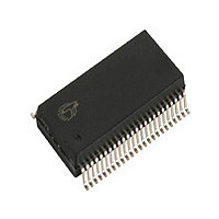
CY7C63413-PVXC Cypress Semiconductor Corp, CY7C63413-PVXC Datasheet - Page 26

CY7C63413-PVXC
Manufacturer Part Number
CY7C63413-PVXC
Description
Manufacturer
Cypress Semiconductor Corp
Datasheet
1.CY7C63413-PVXC.pdf
(32 pages)
Specifications of CY7C63413-PVXC
Cpu Family
enCoRe II
Device Core
M8C
Device Core Size
8b
Frequency (max)
12MHz
Interface Type
USB
Program Memory Type
EPROM
Program Memory Size
8KB
Total Internal Ram Size
256Byte
# I/os (max)
24
Number Of Timers - General Purpose
1
Operating Supply Voltage (typ)
5V
Operating Supply Voltage (max)
5.25/5.5V
Operating Supply Voltage (min)
4/4.35V
Instruction Set Architecture
RISC
Operating Temp Range
0C to 70C
Operating Temperature Classification
Commercial
Mounting
Surface Mount
Pin Count
48
Package Type
SSOP
Lead Free Status / Rohs Status
Compliant
DC Characteristics
Switching Characteristics
Notes:
Document #: 38-08027 Rev. *B
10. Measured as largest step size vs. nominal according to measured full scale and zero programmed values.
11. T
12. Irange: Isinkn(15)/ Isinkn(0) for the same pin.
13. Measured at crossover point of differential data signals.
14. Limits total bus capacitance loading (C
15. DAC I/O Port not bonded out on CY7C63613C. See note on page 12 for firmware code needed for unused pins.
V
I
I
I
R
I
I
I
I
I
I
t
T
9. Per Table 7-7 of revision 1.1 of USB specification, for C
t
t
t
t
t
t
t
t
V
t
t
t
t
t
t
t
t
t
ol
ol
oh
sink0(0)
sink0(F)
sink1(0)
sink1(F)
range
lin
sink
Parameter
CYC
CH
CL
r
r
f
f
rfm
drate
djr1
djr2
deop
eopr1
eopr2
eopt
udj1
udj2
ratio
H
up
Clock
USB Driver Characteristics
USB Data Timing
crs
ratio
= Isink1[1:0](n)/Isink0[7:2](n) for the same n, programmed.
Input Hysteresis Voltage
Sink Current
Sink Current
Source Current
Pull-up Resistance
DAC[7:2] Sink Current (0)
DAC[7:2] Sink Current (F)
DAC[1:0] Sink Current (0)
DAC[1:0] Sink Current (F)
Programmed Isink Ratio: max/min
Differential Nonlinearity
Current Sink Response Time
Tracking Ratio DAC[1:0] to DAC[7:2]
Input Clock Cycle Time
Clock HIGH Time
Clock LOW Time
Transition Rise Time
Transition Rise Time
Transition Fall Time
Transition Fall Time
Rise/Fall Time Matching
Output Signal Crossover Voltage
Low Speed Data Rate
Receiver Data Jitter Tolerance
Receiver Data Jitter Tolerance
Differential to EOP Transition Skew
EOP Width at Receiver
EOP Width at Receiver
Source EOP Width
Differential Driver Jitter
Differential Driver Jitter
Description
Fosc = 6 MHz; Operating Temperature = 0 to 70°C (continued)
DAC Interface
Parameter
LOAD
) to 400 pF per section 7.1.5 of revision 1.1 of USB specification.
[15]
[15]
[15]
[15]
LOAD
of 50–600 pF.
0.45 t
0.45 t
1.4775
165.0
–150
Min.
1.25
–75
–45
–40
330
675
–95
1.3
75
75
80
CYC
CYC
Min.
8.0K
6%
7.2
3.5
1.4
0.1
0.5
1.6
14
8
4
1.5225
168.3
Max.
1.50
300
300
125
100
150
2.0
75
45
95
20.0K
Max.
12%
16.5
10.6
7.5
0.3
1.5
4.8
0.5
0.8
24
21
6
Unit
Mbs
ns
ns
ns
ns
ns
ns
ns
ns
ns
ns
ns
ns
µs
ns
ns
%
Ohms
V
Unit
V
mA
mA
mA
mA
mA
mA
mA
lsb
µs
CC
CLoad = 50 pF
CLoad = 600 pF
CLoad = 50 pF
CLoad = 600 pF
t
Notes 5 and 9
Ave. Bit Rate (1.5 Mb/s ± 1.5%)
To Next Transition
For Paired Transitions
Note 6
Rejects as EOP
Accepts as EOP
To next transition, Figure 12
To paired transition, Figure 12
r
/t
All ports, HIGH to LOW edge
Port 3, Vout = 1.0V (note 4)
Port 0,1,2, Vout = 2.0V (note 4)
Voh = 2.4V (all ports 0,1,2,3) (note 4)
(note 14)
Vout = 2.0 VDC (note 5)
Vout = 2.0 DC (note 5)
Vout = 2.0 VDC (note 5)
Vout = 2.0 VDC (note 5)
Vout = 2.0 VDC (notes 5,12)
Any pin (note 10)
Full scale transition
Vout = 2.0V (note 11)
f
[5, 9]
Conditions
[5, 9]
[5, 9]
Conditions
[13]
[5, 9]
[13]
5, 9]
[13]
CY7C63413C
CY7C63513C
CY7C63613C
[13]
Page 26 of 32
[+] Feedback


